HT9020A View Datasheet(PDF) - Holtek Semiconductor
Part Name
Description
Manufacturer
HT9020A Datasheet PDF : 12 Pages
| |||
HT9020
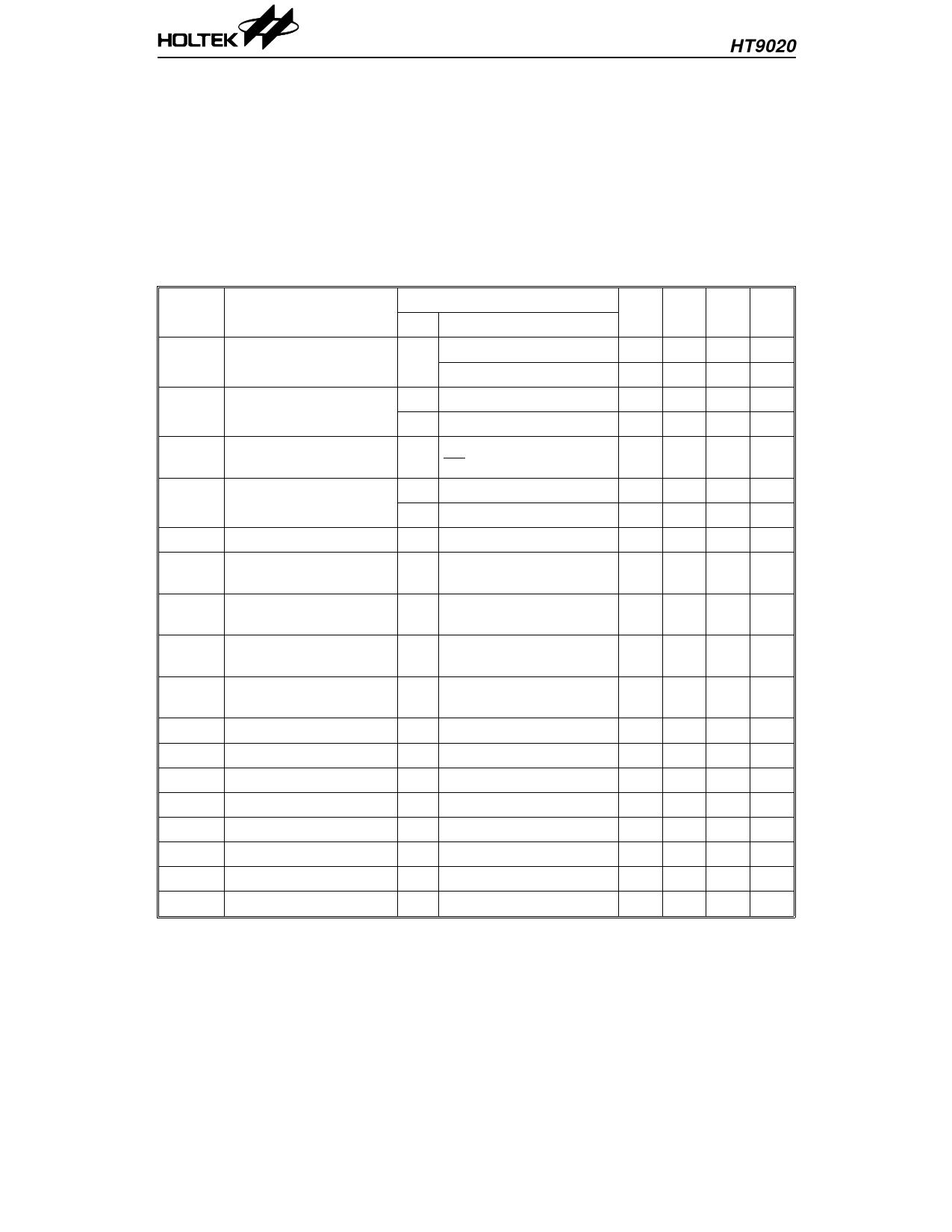
Absolute Maximum Ratings*
Supply Voltage ............................... –0.3V to 6V
Input Voltage ............... VSS–0.3V to VDD+0.3V
Storage Temperature................. –55°C to 150°C
Operating Temperature .............. –20°C to 75°C
*Note: These are stress ratings only. Stresses exceeding the range specified under “Absolute Maxi-
mum Ratings” may cause substantial damage to the device. Functional operation of this
device at other conditions beyond those listed in the specification is not implied and prolonged
exposure to extreme conditions may affect device reliability.
Electrical Characteristics
Symbol
Parameter
Test Conditions
VDD
Conditions
VDD
Operating Voltage
CPT mode
—
ABR mode
IDD
Operating Current
5V Functions enabled
2.5V No load
ISTB
Standby Current
2.5V
Functions disabled or
EN=1
GDV
Detection Level
5V fIN=305~640Hz
2.5V ENV=1
GRL
Rejection Level
— All frequency, ENV=0
fRL
Rejection Out-band
fRH
Frequency
— V≤ 0 dBm, ENV=0
tDD
Detection Signal Time
—
In-band signal input,
ENV=1
tRD
Rejection Noise Time
—
Any signal input,
ENV=0
tDH
Envelope Output
tDL
Delay Time
—
Time to output high
Time to output low
tDV
Data Valid Output Time — Time to output high/low
tSU
Data Setup Time
—
—
tI
Interval Time
— Internal signal
tIP
Interval Pause Time
— Internal signal
tCL
Clear Time
—
—
tST
OSC Start Up Time
—
—
ZI
Input Impedance
— fIN=200~3.4kHz
VREF Reference Voltage
— No load
Min. Typ. Max. Unit
2.5 — 5.5 V
2.0 — 5.5 V
— — 2 mA
— — 0.8 mA
— — 1 µA
–36 — 0 dBm
–42 — –8 dBm
— — –50 dBm
—
800
—
200
—
Hz
40 — — ms
— — 20 ms
— 40 — ms
1.05 1.16 1.2 sec
3
4
5 ms
— 2.32 — sec
8
— ms
— 250 — ns
— 0.8 2 sec
1.0 — — MΩ
2.4 2.5 2.6 V
5
21st Aug ’98
Share Link: 