ICS9248YF-66 View Datasheet(PDF) - Integrated Circuit Systems
Part Name
Description
Manufacturer
ICS9248YF-66 Datasheet PDF : 11 Pages
| |||
ICS9248-66
Advance Information
General Description
The ICS9248-66 is a main clock synthesizer chip for Pentium
II based systems using Rambus Interface DRAMs. This chip
provides all the clocks required for such a system when used
with a Direct Rambus Clock Generator(DRCG) chip such as
the ICS9211-01.
Spread Spectrum may be enabled by driving the SPREAD#
pin active. Spread spectrum typically reduces system EMI
by 8dB to 10dB. This simplifies EMI qualification without
resorting to board design iterations or costly shielding. The
ICS9248-66 employs a proprietary closed loop design, which
tightly controls the percentage of spreading over process
and temperature variations.
The CPU/2 clocks are inputs to the DRCG.
Power Groups:
VDDREF, GNDREF = REF, X1, X2
GNDPCI, VDDPCI = PCICLK
VDD66, GND66 = 3V66
VDD48, GND48 = 48MHz
VDDCOR, GNDCOR = PLL Core
VDDLCPU/2 , GNDLCPU/2 = CPU/2
VDDLIOAPIC, GNDIOAPIC = IOAPIC
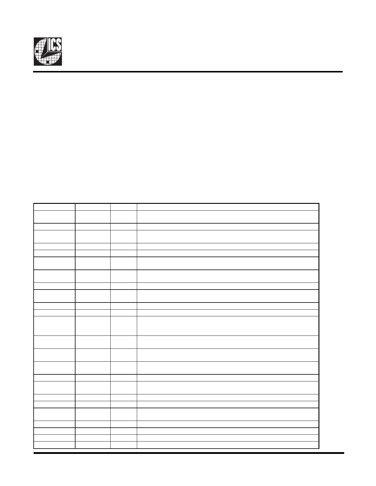
Pin Descriptions
Pin number
1, 7, 13, 19, 23, 26,
35
2, 3
Pin name
GND
REF(0:1)
4, 10, 16, 22, 28, 36
5
6
VDD
X1
X2
8
9, 11, 12, 14,
15, 17, 18
20, 21, 24
PCICLK_F
PCICLK[1:7]
3V66[0:2]
25
27
29, 30
SEL 133/100#
48MHz
SEL[0:1]
31
SPREAD#
32
33
34
40
37, 38, 41
39, 42
43
44
45
46
47
48
PD#
CPU_STOP#
PCI_STOP#
GNDLCPU
CPUCLK[0:3]
VDDLCPU
GNDLCPU/2
CPU/2
VDDLCPU/2
GNDLIOAPIC
IOAPIC
VDDLIOAPIC
Type
PWR
OUT
PWR
IN
OUT
OUT
OUT
OUT
IN
OUT
IN
IN
IN
IN
IN
PWR
OUT
PWR
PWR
OUT
PWR
PWR
OUT
PWR
Description
Ground pins
14.318MHz reference clock outputs at 3.3V
Power pins 3.3V
XTAL_IN 14.318MHz crystal input
XTAL_OUT Crystal output
Free running PCI clock at 3.3V. Synchronous to CPU clocks. Not affected by the
PCI_STOP# input.
PCI clock outputs at 3.3V. Synchronous to CPU clocks.
66MHz outputs at 3.3V. These outputs are stopped when CPU_STOP# is driven active..
This selects the frequency for the CPU and CPU/2 outputs. High = 133MHz,
Low=100MHz
Fixed 48MHz clock output. 3.3V
Function select pins. See truth table for details.
Enables spread spectrum when active(Low). modulates all the CPU, PCI, IOAPIC, 3V66
and CPU/2 clocks. Does not affect the REF and 48MHz clocks. 0.5% down spread
modulation.
This asynchronous input powers down the chip when drive active(Low). The internal PLLs
are disabled and all the output clocks are held at a Low state.
This asychronous input halts the CPUCLK[0:3] and the 3V66[0:3] clocks at logic "0"
when driven active(Low). Does not affect the CPU/2 clocks.
This asynchronous input halts the PCICLK[1:7] at logic"0" when driven active(Low).
PCICLK_F is not affected by this input.
Ground pin for the CPUCLKs
Host bus clock output at 2.5V. 133MHz or 100MHz depending on the state of the SEL
133/100MHz.
Power pin for the CPUCLKs. 2.5V
Ground pin for the CPU/2 clocks.
2.5V clock outputs at 1/2 CPU frequency. 66MHz or50MHz depending on the state of the
SEL 133/100# input pin.
Power pin for the CPU/2 clocks. 2.5V
Ground pin for the IOAPIC outputs.
IOAPIC clocks at 2.5V. Synchronous with CPUCLKs but fixed at 16.67MHz.
Power pin for the IOAPIC outputs. 2.5V.
2
Share Link: 