ICS9250-14 View Datasheet(PDF) - Integrated Circuit Systems
Part Name
Description
Manufacturer
ICS9250-14 Datasheet PDF : 13 Pages
| |||
ICS9250 - 14
Preliminary Product Preview
Absolute Maximum Ratings
Core Supply Voltage . . . . . . . . . . . . . . . . . . . . . . 4.6V
I/O Supply Voltage . . . . . . . . . . . . . . . . . . . . . . . 3.6V
Logic Inputs . . . . . . . . . . . . . . . . . . . . . . . . . . . . GND 0.5 V to VDD +0.5 V
Ambient Operating Temperature . . . . . . . . . . . . 0°C to +70°C
Storage Temperature . . . . . . . . . . . . . . . . . . . . . . 65°C to +150°C
Case Temperature . . . . . . . . . . . . . . . . . . . . . . . . 115°C
Stresses above those listed under Absolute Maximum Ratings may cause permanent damage to the device. These ratings are
stress specifications only and functional operation of the device at these or any other conditions above those listed in the
operational sections of the specifications is not implied. Exposure to absolute maximum rating conditions for extended
periods may affect product reliability.
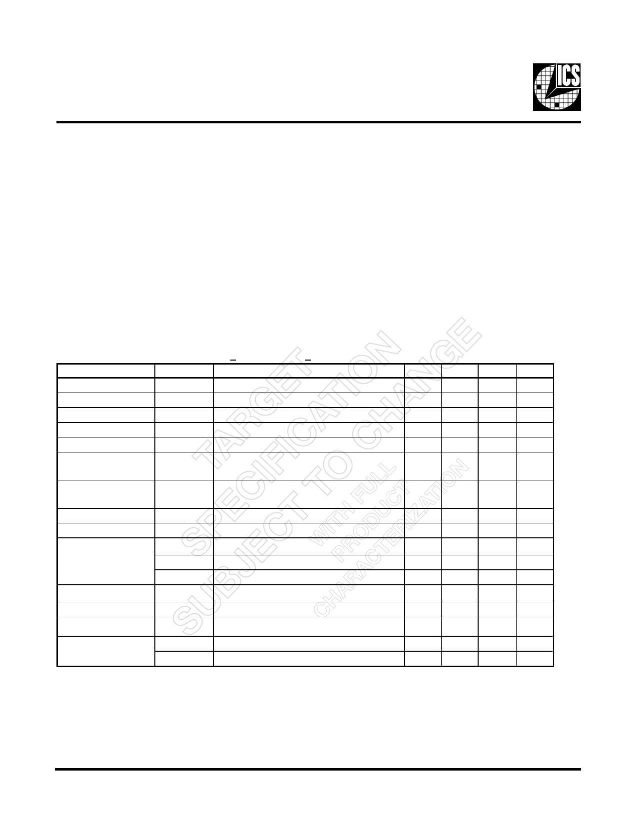
Electrical Characteristics - Input/Supply/Common Output Parameters
TA = 0 - 70C; Supply Voltage VDD = 3.3 V +5%, VDDL=2.5 V+ 5%(unless otherwise stated)
PARAMETER
SYMBOL
CONDITIONS
MIN TYP MAX UNITS
Input High Voltage
VIH
2
VDD+0.3 V
Input Low Voltage
Input High Current
Input Low Current
Input Low Current
VIL
VSS-0.3
0.8
V
IIH
VIN = VDD
-5
5
µA
IIL1 VIN = 0 V; Inputs with no pull-up resistors
-5
2.0
µA
IIL2 VIN = 0 V; Inputs with pull-up resistors
-200 -100
µA
Operating
IDD3.3OP CL = 0 pF; Select @ 66M
60 100 mA
Supply Current
Power Down
IDD3.3PD CL = 0 pF; With input address to Vdd or GND
400 600 µA
Supply Current
Input frequency
Fi
VDD = 3.3 V;
14.318
MHz
Pin Inductance
Input Capacitance1
Lpin
CIN Logic Inputs
7
nH
5
pF
Cout Out put pin capacitance
6
pF
CINX X1 & X2 pins
13.5
Transition Time1
Ttrans To 1st crossing of target Freq.
Settling Time1
Ts
From 1st crossing to 1% target Freq.
Clk Stabilization1
TSTAB From VDD = 3.3 V to 1% target Freq.
22.5 pF
3
mS
mS
3
mS
Delay
tPZH,tPZH output enable delay (all outputs)
1
10
nS
tPLZ,tPZH output disable delay (all outputs)
1
10
nS
1Guarenteed by design, not 100% tested in production.
8
Share Link: 