IDT71216 View Datasheet(PDF) - Integrated Device Technology
Part Name
Description
Manufacturer
IDT71216
Integrated Device Technology

IDT71216 Datasheet PDF : 14 Pages
| |||
IDT71216
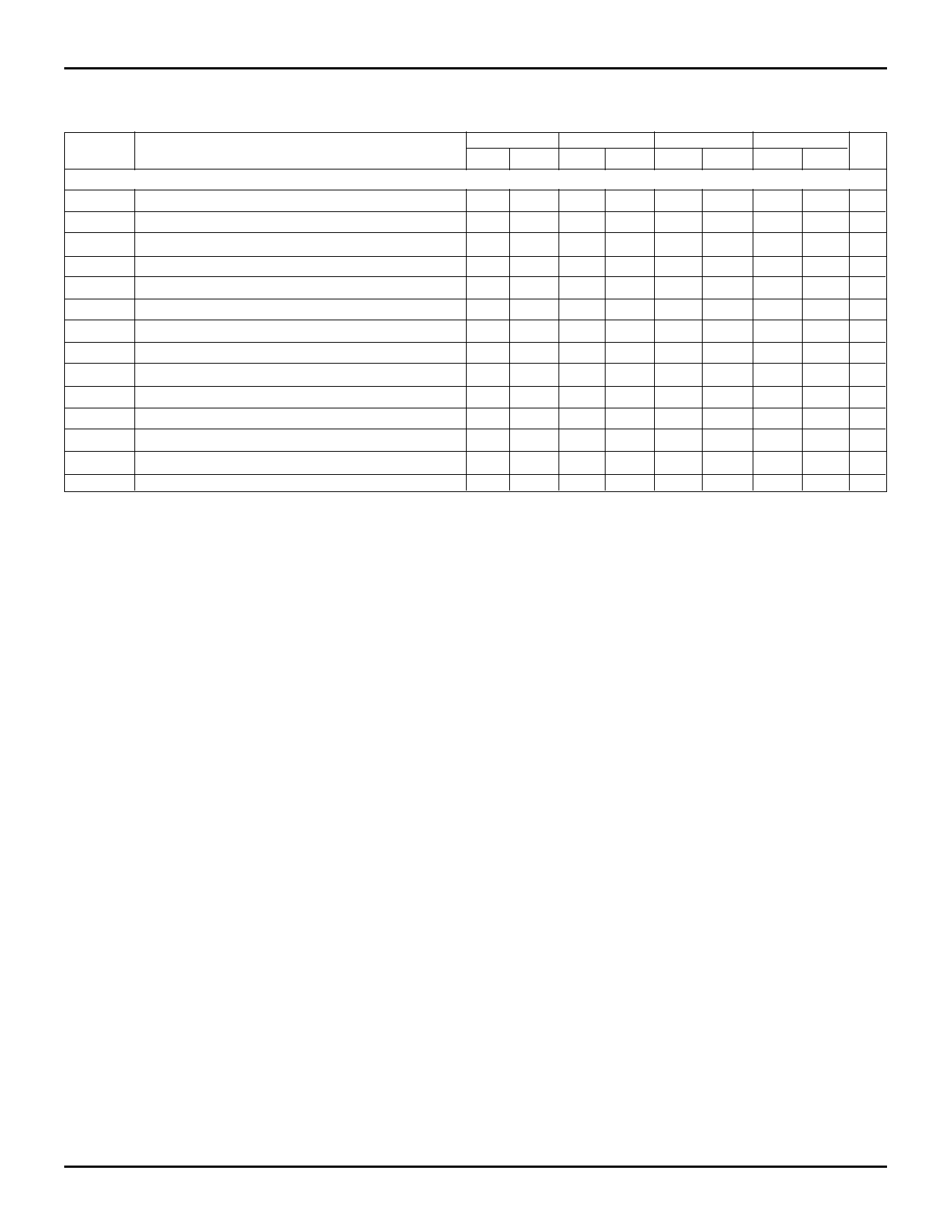
BiCMOS 16K x 15 CACHE-TAG RAM
COMMERCIAL TEMPERATURE RANGE
AC ELECTRICAL CHARACTERISTICS (1)
(VCC = 5.0V ± 5%, VCCQ = 5.0V ± 5% OR 3.3V ± 0.3V, TA = 0 to 70°C)
IDT71216S8
Symbol
Parameter
Min. Max.
IDT71216S9 IDT71216S10
Min. Max. Min. Max.
Write Cycle and Clock Parameters
tCYC Clock Cycle Time
15 —
15 —
15
—
tCH(2, 3) Clock Pulse HIGH
4.5 —
tCL(2, 3) Clock Pulse LOW
4.5 —
tS
WET, WES, Chip Select, and Input Data Set-up Time 3 —
tH
WET, WES, Chip Select, and Input Data Hold Time
1—
4.5 — 4.5 —
4.5 — 4.5 —
3—
3
—
1—
1
—
tSA Address Set-up Time
3—
3—
3
—
tHA Address Hold Time
tWMI CLK HIGH Write to MATCH and TA Invalid
1—
—6
1—
1
—
—7
—
7
tCKLZ(3) CLK HIGH Read to Outputs in Low-Z
1.5 —
1.5 — 1.5 —
tCTV(4)
tCSV(4)
CLK HIGH Read to Tag Bits Valid
CLK HIGH Write to Status Outputs Valid
—9
—8
— 10
—
10
—9
—
9
tCSH(3)
tWHPL
tPUWL
Status Output Hold from CLK HIGH Write
WET and WES HIGH to PWRDN LOW
PWRDN HIGH to WET and WES Active
0—
5—
50 —
0—
0
—
5—
5
—
50 —
50
—
NOTES:
1. All Write cycles are synchronous and referenced from rising CLK.
2. This parameter is measured as a HIGH time above 2.0V and a LOW time below 0.8V.
3. This parameter is guaranteed with the AC Load (Figure 3) by device characterization, but is not production tested.
4. Addresses are stable prior to CLK transition HIGH.
IDT71216S12
Min. Max. Unit
16.6
5
5
3
1
3
1
—
1.5
—
—
0
5
50
— ns
— ns
— ns
— ns
— ns
— ns
— ns
8 ns
— ns
12 ns
10 ns
— ns
— ns
— ns
3067 tbl 14
14.3
8
Share Link: