IDT71V016S20PH View Datasheet(PDF) - Integrated Device Technology
Part Name
Description
Manufacturer
IDT71V016S20PH Datasheet PDF : 9 Pages
| |||
IDT71V016, 3.3V CMOS Static RAM
1 Meg (64K x 16-Bit)
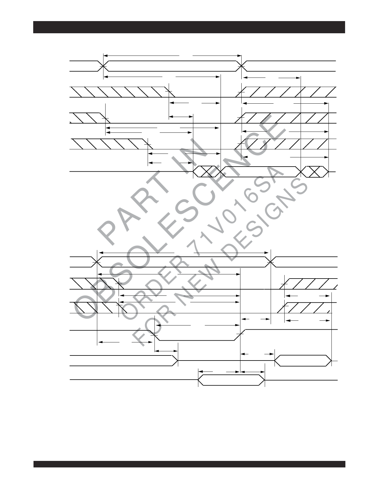
Timing Waveform of Read Cycle No. 2(1)
Commercial and Industrial Temperature Ranges
ADDRESS
tRC
tAA
tOH
OE
(3)
tOE
tOHZ
(3)
tOLZ
CS
E BHE, BLE
N C DATAOUT
tCLZ (3) tACS (2)
tBE (2)
(3)
tBLZ
(3)
tCHZ
(3)
tBHZ
DATA OUT VALID
T I EN A NOTES:
S S 1. WE is HIGH for Read Cycle.
R C 6 2. Address must be valid prior to or coincident with the later of CS, BHE, or BLE transition LOW; otherwise tAA is the limiting parameter.
1 N 3. Transitionismeasured±200mVfromsteadystate.
3211 drw 08
PA ES V0 SIG Timing Waveform of Write Cycle No. 1 (WE Controlled Timing)(1,2,4)
L 71 DE ADDRESS
SO ER W CS
B RD NE BHE, BLE
O OFOR WE
tWC
tAW
tCW (2)
tBW
tWP
tAS
tWHZ (5)
(5)
tCHZ
tWR
(5)
tBHZ
(5)
tOW
DATAOUT
PREVIOUS DATA VALID (3)
DATA VALID
tDH
tDW
DATAIN
DATAIN VALID
3211 drw 09
NOTES:
1. A write occurs during the overlap of a LOW CS, LOW BHE or BLE, and a LOW WE.
2. OE is continuously HIGH. If during a WE controlled write cycle OE is LOW, tWP must be greater than or equal to tWHZ + tDW to allow the I/O drivers to turn off and data to be placed
on the bus for the required tDW. If OE is HIGH during a WE controlled write cycle, this requirement does not apply and the minimum write pulse is as short as the specified tWP.
3. During this period, I/O pins are in the output state, and input signals must not be applied.
4. If the CS LOW or BHE and BLE LOW transition occurs simultaneously with or after the WE LOW transition, the outputs remain in a high-impedance state.
5. Transition is measured ±200mV from steady state.
6.462
Share Link: 