IR1176 View Datasheet(PDF) - International Rectifier
Part Name
Description
Manufacturer
IR1176 Datasheet PDF : 12 Pages
| |||
IR1176
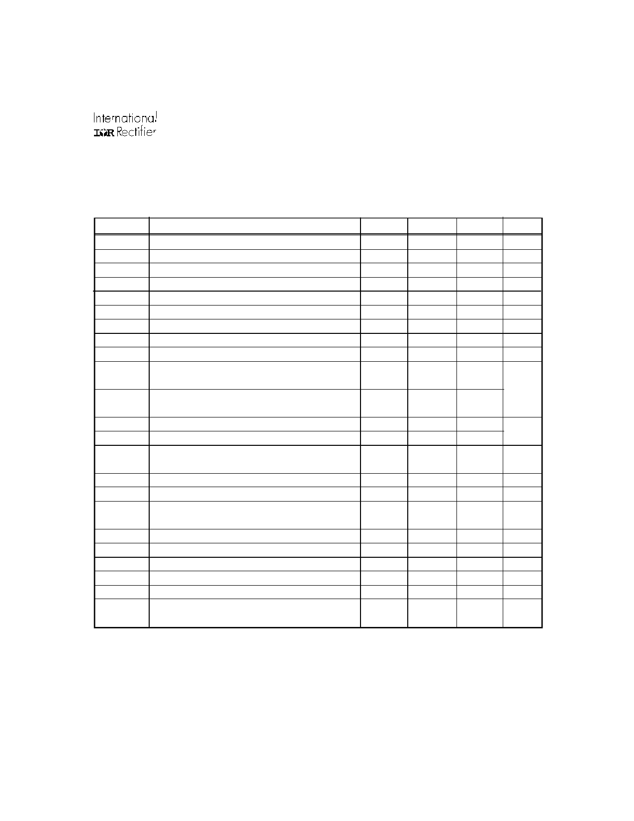
Dynamic Electrical Characteristics
Vdd=5V, TA = 25oC, Rbias = 34.0K unless otherwise specified.
Symbol Definition
Vdd
Iqdd
Supply voltage operating range
Vdd quiescent current (x1 = x2 = 0V or 5V, Iout = 0)
Freq
UVSET+
Operating frequency
UVSET positive going threshold
UVSET-
Vxth+
UVSET negative going threshold
X1/X2 Input positive going threshold
Vxth-
Tadv
X1/X2 Input negative going threshold
Externally adjustable lead time (advance)
Td
Isink
Externally adjustable dead-time for Q1 and Q2
Q1,Q2 output sink current (Vdd=5.0V,
(peak)
Isource
pulsed, 10 usec)
Q1,Q2 output source current (Vdd=5.0V,
(peak)
VOH
pulsed, 10 usec)
Q1, Q2 High level voltage (Iout = 20mA)
VOL
tio
Q1, Q2 Low level voltage (Iout = 20mA)
Input to output delay (PLL bypassed, cross coupled
mode)
tr
Gate turn-on rise time (C1=1000pf, Vdd=5V)
tf
Gate turn-off fall time (C1=1000pf, Vdd=5V)
Vtr
Cross-over voltage (Vdd=5Vdc, DTIN shorted to
Rbias
DTOUT, C1=1000pf) Fig. 3
Required bias resistor (1%)
Vbias
Tjitter
Voltage at Rbias pin
Phase-lock loop output jitter
Ichgpump Charge pump output current (at VFLTR pin)
Vchgpump Charge pump output voltage (at VFLTR pin)
Kvco_dc PLL Vco DC gain (per design)
Min.
4.0
—
100
1.10
0.8
—
—
—
20
—
—
—
—
—
—
—
—
—
—
-20
—
1.3
—
Typ.
—
4
—
—
—
1.4
1.0
—
—
4
Max.
5.25
5
2000
1.4
1.1
—
—
500
—
—
4
—
Vdd- 0.20
—
0.10
—
20
—
20
—
20
—
2.5
—
34.0
—
1.25
—
—
20
50
—
1.5
1.7
62
—
Units
VDC
A
KHz
V
V
VDC
VDC
nsec
nsec
A
V
nsec
nsec
nsec
VDC
KΩ
VDC
nsec
µA DC
VDC
KHz/
Volt
www.irf.com
3
Share Link: 