LE28F4001M View Datasheet(PDF) - SANYO -> Panasonic
Part Name
Description
Manufacturer
LE28F4001M Datasheet PDF : 14 Pages
| |||
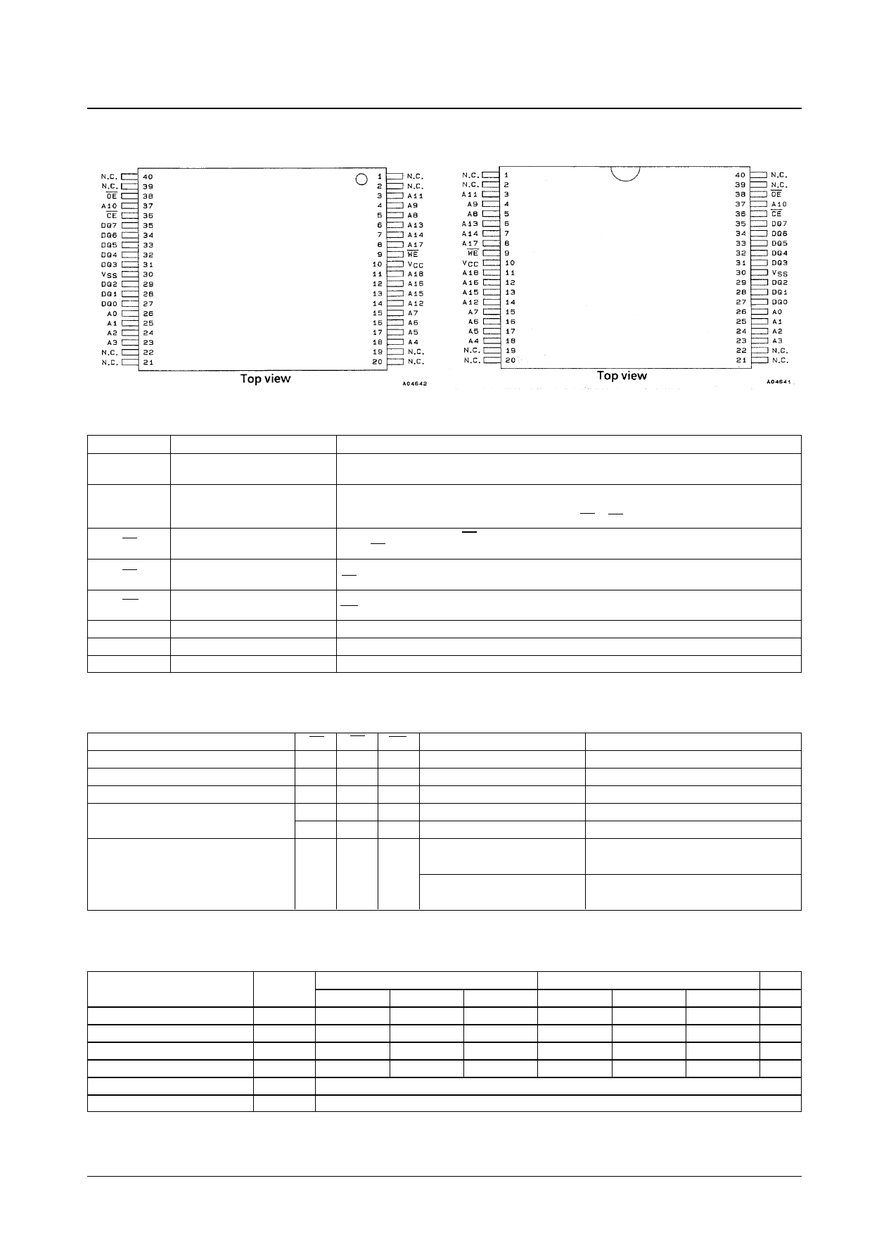
TSOP40 Standard
LE28F4001M, T, R-15/20
TSOP40 Reversed
Pin Functions
Symbol
A18 to A0
Pin
Address input
DQ7 to DQ0 Data input and output
CE
OE
WE
VCC
VSS
N.C.
Chip enable
Output enable
Write enable
Power supply
Ground
No connection
Functions
Supply the memory address to these pins.
The address is latched internally during a write cycle.
These pins output data during a read cycle and input data during a write cycle.
Data is latched internally during a write cycle.
Outputs go to the high-impedance state when either OE or CE is high.
The device is active when CE is low.
When CE is high, the device becomes unselected and goes to the standby state.
Makes the data output buffers active.
OE is a low-active input.
Makes the write operation active.
WE is a low-active input.
Apply 5 V (В±10%) to this pin.
These pins must be left open.
Function Logic
Mode
Read
Write
Standby or write inhibit
Write inhibit
Product identification
CE
OE
WE
A18 to A0
DQ7 to DQ0
VIL
VIL
VIH AIN
VIL
VIH
VIL AIN
VIH
X
XX
X
VIL
XX
X
X
VIH X
DOUT
DIN
High-Z
High-Z/DOUT
High-Z/DOUT
A18 to A10 = VIL, A8 to A1 = VIL, Manufacturer code (BF)
A9 = 12 V, A0 = VIL
VIL
VIL
VIH
A18 to A10 = VIL, A8 to A1 = VIL Device code (04)
A9 = 12 V, A0 = VIH
Command Settings
Command
Sector erase
Byte program
Reset
Read ID
Software data unprotect
Software data protect
Request
cycle
2
2
1
3
7
7
Setup command cycle
Operation
Address
Write
X
Write
X
Write
X
Write
X
See Figure 9.
See Figure 10.
Data
20H
10H
FFH
90H
Execute command cycle
Operation
Address
Data
Write
SA
D0H
Write
PA
PD
Read
(7)
(7)
SDP
N
N
Y
Y
No. 5239-3/14
Share Link: 