IS61C64AH View Datasheet(PDF) - Integrated Circuit Solution Inc
Part Name
Description
Manufacturer
IS61C64AH Datasheet PDF : 8 Pages
| |||
IS61C64AH
WRITE CYCLE SWITCHING CHARACTERISTICS(1,3) (Over Operating Range)
Symbol Parameter
-12 ns
Min. Max.
-15 ns
Min. Max.
-20 ns
Min. Max.
-25 ns
Min. Max. Unit
tWC Write Cycle Time
tSCE1 CE1 to Write End
12 —
10 —
15 —
12 —
20 —
17 —
25 —
ns
22 —
ns
tSCE2 CE2 to Write End
10 —
12 —
17 —
22 —
ns
tAW Address Setup Time to Write End 10 —
12 —
15 —
20 —
ns
tHA Address Hold from Write End
0—
0—
0—
0—
ns
tSA Address Setup Time
t (4)
PWE
WE Pulse Width
0—
8—
0—
10 —
0—
12 —
0—
ns
15 —
ns
tSD Data Setup to Write End
8—
9—
10 —
12 —
ns
tHD
t (2)
HZWE
t (2)
LZWE
Data Hold from Write End
WE LOW to High-Z Output
WE HIGH to Low-Z Output
0—
—6
0—
0—
—8
0—
0—
— 10
0—
0—
ns
— 12
ns
0—
ns
Notes:
1. Test conditions assume signal transition times of 5 ns or less, timing reference levels of 1.5V, input pulse levels of 0 to 3.0V
and output loading specified in Figure 1.
2. Tested with the load in Figure 2. Transition is measured ±500 mV from steady-state voltage. Not 100% tested.
3. The internal write time is defined by the overlap of CE1 LOW, CE2 HIGH and WE LOW. All signals must be in valid states to
initiate a Write, but any one can go inactive to terminate the Write. The Data Input Setup and Hold timing are referenced to the
rising or falling edge of the signal that terminates the write.
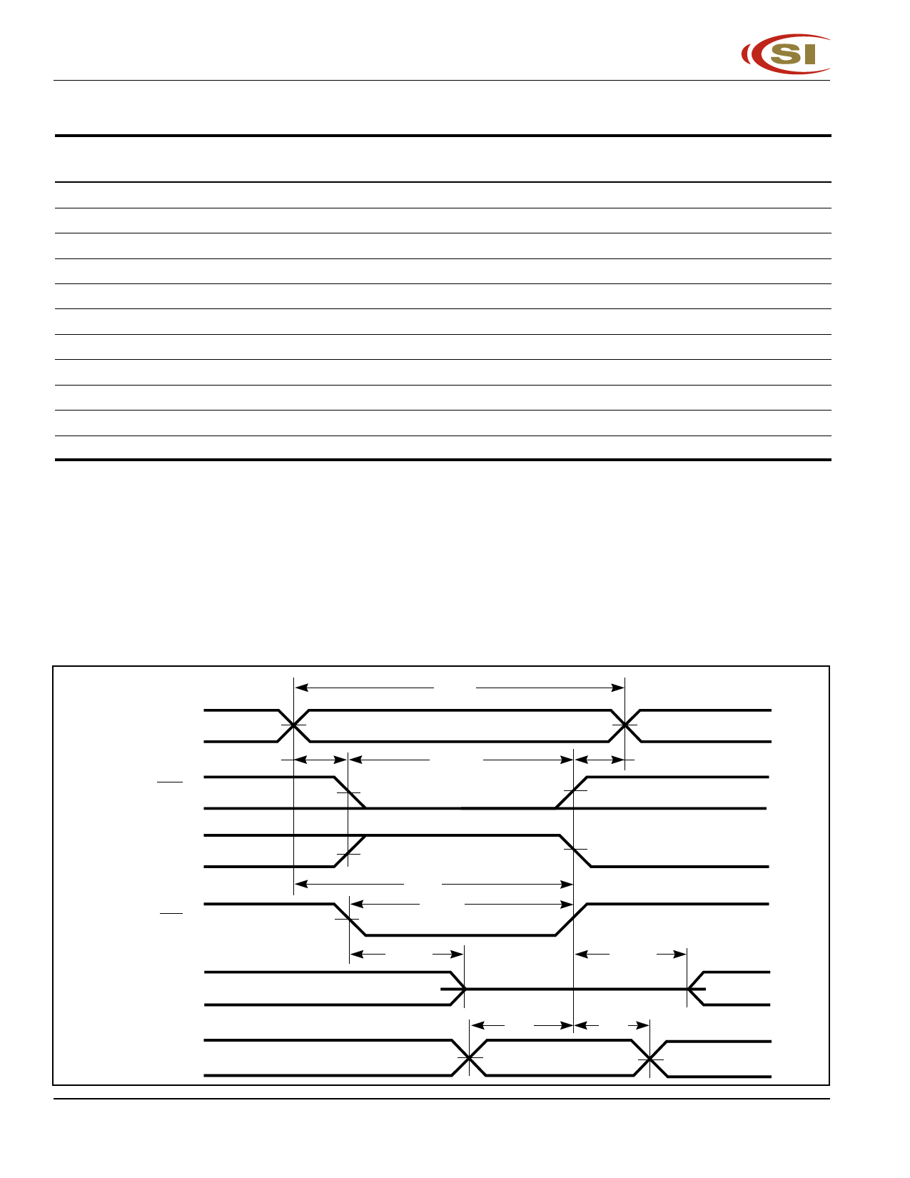
AC WAVEFORMS
WRITE CYCLE NO. 1 (CE Controlled, OE is HIGH or LOW) (1 )
t WC
ADDRESS
t SA
CE1
VALID ADDRESS
t SCE1
t SCE2
t HA
CE2
WE
DOUT
DIN
DATA UNDEFINED
t AW
t PWE1
t PWE2
t HZWE
HIGH-Z
t LZWE
t SD
t HD
DATAIN VALID
6
Integrated Circuit Solution Inc.
SR001-B
Share Link: 