K6R1016V1D-JC08(2001) View Datasheet(PDF) - Samsung
Part Name
Description
Manufacturer
K6R1016V1D-JC08 Datasheet PDF : 11 Pages
| |||
K6R1016V1D
for AT&T
CMOS SRAM
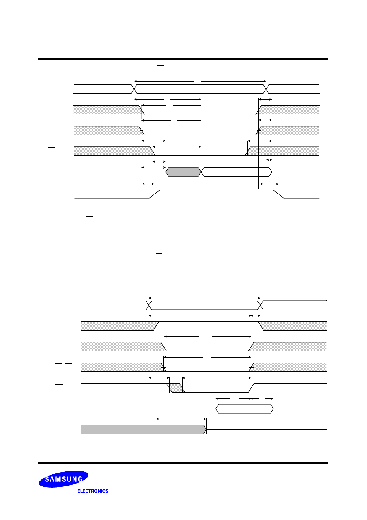
TIMING WAVEFORM OF READ CYCLE(2) (WE=VIH)
Address
CS
UB, LB
OE
Data out
High-Z
tRC
tAA
tCO
tBA
tBLZ(4,5)
tOE
tOLZ
tLZ(4,5)
VCC
ICC
Current
ISB
tPU
50%
tHZ(3,4,5)
tBHZ(3,4,5)
tOHZ
Valid Data
tPD
50%
NOTES(READ CYCLE)
1. WE is high for read cycle.
2. All read cycle timing is referenced from the last valid address to the first transition address.
3. tHZ and tOHZ are defined as the time at which the outputs achieve the open circuit condition and are not referenced to VOH or
VOL levels.
4. At any given temperature and voltage condition, tHZ(Max.) is less than tLZ(Min.) both for a given device and from device to
device.
5. Transition is measured ±200mV from steady state voltage with Load(B). This parameter is sampled and not 100% tested.
6. Device is continuously selected with CS=VIL.
7. For common I/O applications, minimization or elimination of bus contention conditions is necessary during read and write cycle.
TIMING WAVEFORM OF WRITE CYCLE(1) (OE =Clock)
Address
OE
CS
UB, LB
WE
Data in
Data out
tWC
tAW
tCW(3)
tWR(5)
tBW
tAS(4)
tWP(2)
High-Z
tOHZ(6)
tDW
tDH
Valid Data
High-Z
-7-
Revision 1.0
December 2001
Share Link: 