76105SK8 View Datasheet(PDF) - Fairchild Semiconductor
Part Name
Description
Manufacturer
76105SK8 Datasheet PDF : 12 Pages
| |||
HUF76105SK8
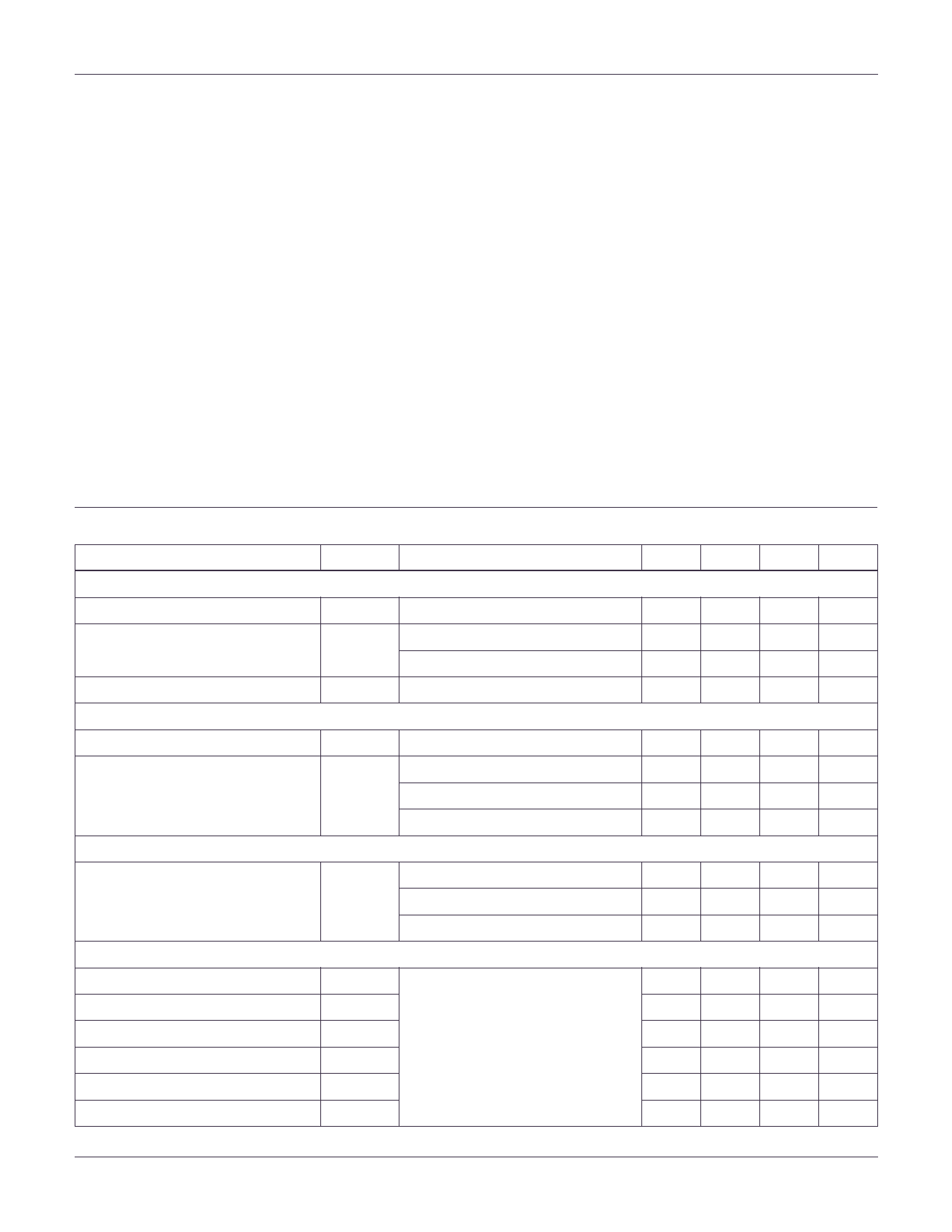
Absolute Maximum Ratings TA = 25oC, Unless Otherwise Specified
UNITS
Drain to Source Voltage (Note 1) . . . . . . . . . . . . . . . . . . . . . . . . . . . . . . . . . . . . . . . . . . VDSS
30
V
Drain to Gate Voltage (RGS = 20kΩ) (Note 1) . . . . . . . . . . . . . . . . . . . . . . . . . . . . . . . . VDGR
30
V
Gate to Source Voltage . . . . . . . . . . . . . . . . . . . . . . . . . . . . . . . . . . . . . . . . . . . . . . . . . . VGS
±20
V
Drain Current
Continuous
Continuous
Continuous
(TA=
(TA=
(TA=
211500o00CooCC, V,, VVGGGSSS===1540V.V5))V(()FN(ioNgtueorte3e)23.)).(..N..o..te.. ..2..)..
.
.
.
.
.
.
.
.
.
.
.
.
.
.
.
.
.
.
.
.
.
.
.
.
.
.
.
.
.
.
.
.
.
.
.
.
.
.
.
.
.
.
.
.
.
.
.
.
.
.
.
.
.
.
.
.
.
.
.
.
.
.
.
.
.
.
.
.
.
.
.
.
.
.
.
ID
ID
ID
Pulsed Drain Current . . . . . . . . . . . . . . . . . . . . . . . . . . . . . . . . . . . . . . . . . . . . . . . . . . .IDM
5.5
A
1.4
A
1.3
A
Figure 4
Pulsed Avalanche Rating . . . . . . . . . . . . . . . . . . . . . . . . . . . . . . . . . . . . . . . . . . . . . . . . . EAS
Figures 6, 17, 18
Power Dissipation (Note 2)
Derate Above 25oC . . . .
.
.
.
.
.
.
.
.
.
.
.
.
.
.
.
.
.
.
.
.
.
.
.
.
.
.
.
.
.
.
.
.
.
.
.
.
.
.
.
.
.
.
.
.
.
.
.
.
.
.
.
.
.
.
.
.
.
.
.
.
.
.
.
.
.
.
.
.
.
.
.
.
.
.
.
.
.
.
.
.
.
.
.
.
.
.
.
.
.
.
.
.
.
.
.
.
PD
...
2.5
W
20
mW/oC
Operating and Storage Temperature . . . . . . . . . . . . . . . . . . . . . . . . . . . . . . . . . . . . TJ, TSTG
-55 to 150
oC
Maximum Temperature for Soldering
Leads at 0.063in (1.6mm) from Case for 10s . . . . . . . . . . . . . . . . . . . . . . . . . . . . . . . . . . TL
Package Body for 10s, See Techbrief 334 . . . . . . . . . . . . . . . . . . . . . . . . . . . . . . . . . . Tpkg
300
oC
260
oC
CAUTION: Stresses above those listed in “Absolute Maximum Ratings” may cause permanent damage to the device. This is a stress only rating and operation of the
device at these or any other conditions above those indicated in the operational sections of this specification is not implied.
NOTES:
1. TJ = 25oC to 125oC.
2. 50oC/W measured using FR-4 board at 1 second.
3. 212oC/W measured using FR-4 board with 0.0115 in2 copper pad at 1000 seconds.
Electrical Specifications TA = 25oC, Unless Otherwise Specified
PARAMETER
SYMBOL
TEST CONDITIONS
MIN
TYP
MAX UNITS
OFF STATE SPECIFICATIONS
Drain to Source Breakdown Voltage
Zero Gate Voltage Drain Current
Gate to Source Leakage Current
ON STATE SPECIFICATIONS
BVDSS
IDSS
IGSS
ID = 250µA, VGS = 0V (Figure 12)
VDS = 25V, VGS = 0V
VDS = 25V, VGS = 0V, TC = 150oC
VGS = ±20V
30
-
-
V
-
-
1
µA
-
-
250
µA
-
-
±100
nA
Gate to Source Threshold Voltage
Drain to Source On Resistance
THERMAL SPECIFICATIONS
Thermal Resistance Junction to Ambient
VGS(TH)
rDS(ON)
VGS = VDS, ID = 250µA (Figure 11)
ID = 5.5A, VGS = 10V (Figures 9, 10)
ID = 1.4A, VGS = 5V (Figure 9)
ID = 1.3A, VGS = 4.5V (Figure 9)
RθJA
Pad Area = 0.76 in2 (Note 2)
Pad Area = 0.054 in2 (Figure 23)
Pad Area = 0.0115 in2 (Figure 23)
1
-
3
V
-
0.040 0.050
Ω
-
0.055 0.072
Ω
-
0.060 0.078
Ω
-
-
50
oC/W
-
-
175
oC/W
-
-
212
oC/W
SWITCHING SPECIFICATIONS (VGS = 4.5V)
Turn-On Time
tON
Turn-On Delay Time
td(ON)
Rise Time
tr
Turn-Off Delay Time
td(OFF)
Fall Time
tf
Turn-Off Time
tOFF
VDD = 15V, ID ≅ 1.3A, RL = 11.5Ω,
VGS = 4.5V, RGS = 27Ω
(Figures 15, 21, 22)
-
-
60
ns
-
12
-
ns
-
28
-
ns
-
31
-
ns
-
21
-
ns
-
-
80
ns
©2003 Fairchild Semiconductor Corporation
HUF76105SK8 Rev. B1
Share Link: 