L9524C-TR View Datasheet(PDF) - STMicroelectronics
Part Name
Description
Manufacturer
L9524C-TR Datasheet PDF : 27 Pages
| |||
L9524C
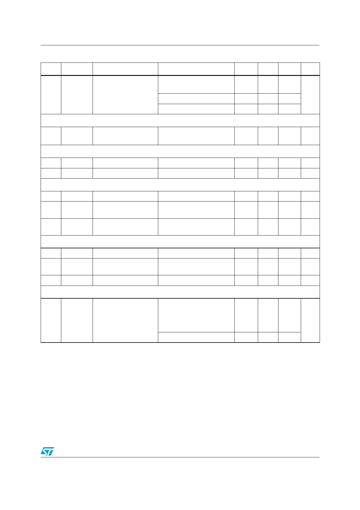
Table 5. Electrical characteristics (continued)
Item Symbol
Parameter
Test condition
11.2 RSN1-6 Pull down resistor
6V ≤ VSNX = VSPX ≤ 20V
-40°C
35°C
125°C
Overcurrent threshold setting (OCT)
12.1
IOCT Input pull-up current
VVS ≥ 6V
VOCT = 3.5V
Power MOSFET gate charge/discharge current setting (CUR)
13.1
13.2
VCUR
ICUR max
Output voltage
Current limitation
Input pin for mode selection (MS)
ICUR ≥ -150μA
VCUR ≤ 2V
14.1
IMS
Pull-up current
14.2
VMS tr
Transistor mode
threshold
VMS = 3V
14.3
VMS tc
Temperature
compensation threshold
VVS ≥ 6V
Output timing
15.1
tdel
15.2
tgap
Delay time (2)
Gap between channels
(2)
15.3
tsup
Power regulation
Failure suppress time (2)
16.1
ΔVRMS Accuracy
8V ≤ VBAT ≤ 16V
30ms ≤ TCI ≤ 33ms
tCI on/TCI ≥ 20%
< 70°C
> 70°C
1. not tested, guaranteed by design
2. time constants created digitally, verified by scan path test
Electrical specifications
Min. Typ. Max. Unit
40
100 270
kΩ
40
150 270
40
220 270
-40
-10 μA
2.35 2.5 2.65 V
-500
-250 μA
-60
-15 μA
1
2
V
3
4
V
2.5
5
ms
50
250 μs
400
950 μs
-1.5
1.5% % ·
VRMSref
-2
2
11/27
Share Link: 