LB1851M View Datasheet(PDF) - SANYO -> Panasonic
Part Name
Description
Manufacturer
LB1851M Datasheet PDF : 6 Pages
| |||
LB1851M
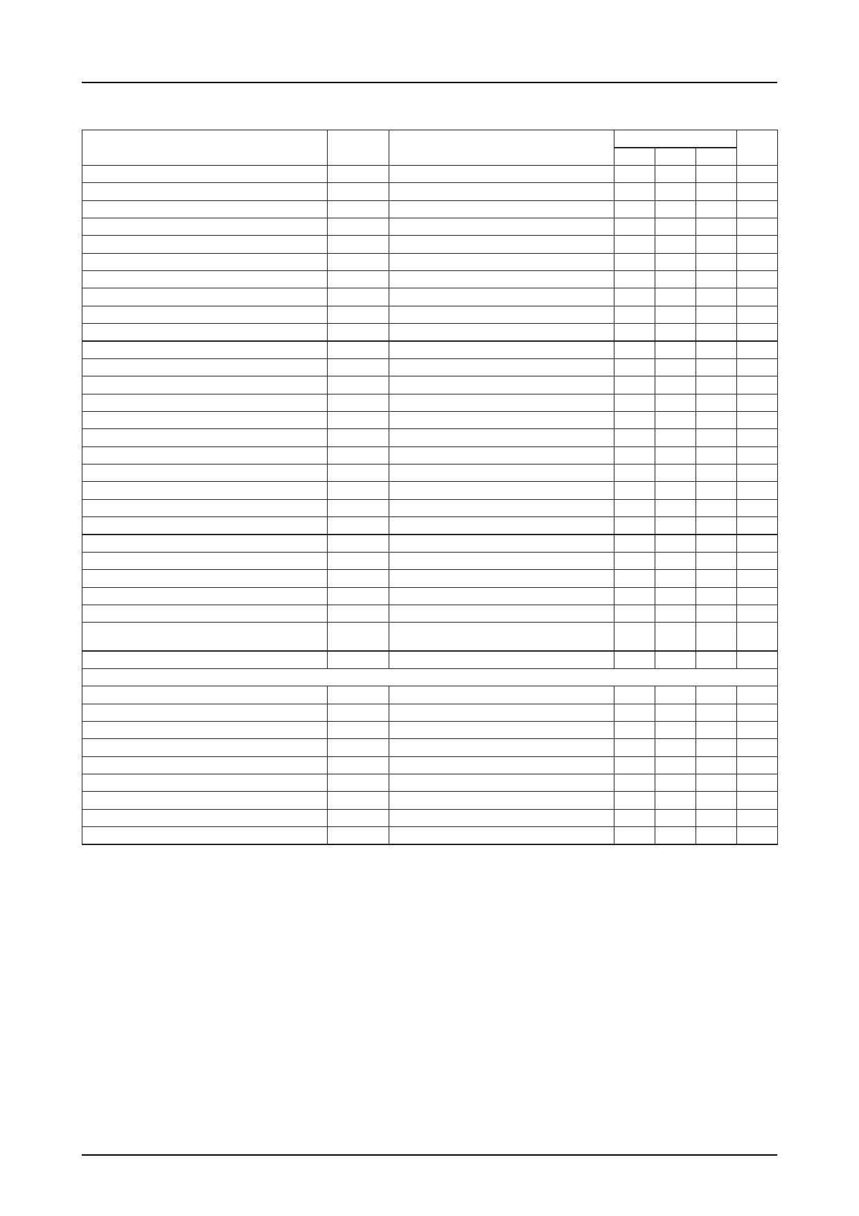
Electrical Characteristics at Ta = 25˚C, VCC1=5V, VCC2=7V, VS=3V
Parameter
Symbol
Conditions
Ratings
Unit
min typ max
Supply current 1
Supply current 2
Supply current 3
Output standby current 1
Output standby current 2
Output saturation voltage
Output TRS voltage
Output standby voltage
Hall amplifier input Offset votlage
Hall amplifier common-mode Input voltage range
Hall input-output Voltage gain
Brake pin 'H'-level voltage
ICC1
ICC2
IS
ICCOQ
ISOQ
VO(sat)
VO(sus)
VOQ
VH offset
VHCOM
GVHO
VBR=5V
VBR=5V
VBR=5V, RL=∞
VSTBY=0V
VSTBY=0V, RL=∞
IOUT=1.0A, sink+source
IOUT=20mA
IBR=5V
Rangle=8.2kΩ
4.5 6.5 mA
15
20 mA
6.5 9.0 mA
180 µA
150 µA
2.3 V
16
V*
1.4 1.5 1.6 V
–5
+5 mV*
1.4
2.8 V
31.5 34.5 37.5 dB
2.0
V
Brake pin 'L'-level voltage
0.8 V
Brake pin input current
100 µA
Brake pin leakage current
–30 µA
FRC pin 'H'-level voltage
2.8
V
FRC pin 'L'-level voltage
1.2 V
FRC pin input current
100 µA
FRC pin leakage current
–30 µA
Upper residual voltage
Lower residual voltage
Residual voltage inflection point
VXH IOUT=100mA, VCC2=6V, VS=2V
VXL IOUT=100mA, VCC2=6V, VS=2V
0.38
0.55 V
0.41
0.5 V
2.0
V
Overlap amount
Standby ON voltage
VCC2=6V, VS=3V
60
70
80 %
–0.2
+0.1 V
Standby OFF voltage
Open : standby off (note1)
2
5V
Standby pin bias current
Pin GND
10 µA
Operating temperature of
thermal shutdown circuit
Hysteresis of thermal shutdown circuit
[FG Amplifier]
150 180 210
˚C*
15
˚C*
FG amplifier input offset voltage
Open loop voltage gain
Source side output saturation voltage
Sink side output saturation voltage
Common-mode signal rejection
VFG offset
GVFG
VFG OUT
VFG OD
CHR
f=1kHz
IO=–2mA
IO=2mA
–8
+8 mV
60
dB
3.7
V
1.3 V
80
dB*
FG ampilier common-mode input voltage range
Phase margin
Schmitt amplifier threshold voltage
Schmitt amplifier hysteresis
VFG CH
VFG in+=2.5V, VFGOUT2 at H to L
VFG in+=2.5V
0
3.5 V
20
˚C*
2.45 2.50 2.55 V
20
40
60 mV
Note1 : When standby pin is left open, standby operation is turned to off.
Note2*: Values shown are design targets only. No measurements have been taken. Overlap spec. are regarded as test
specification.
No.3659-2/6
Share Link: 