LC6513A(2001) View Datasheet(PDF) - SANYO -> Panasonic
Part Name
Description
Manufacturer
LC6513A
(Rev.:2001)
(Rev.:2001)
SANYO -> Panasonic

LC6513A Datasheet PDF : 24 Pages
| |||
LC6512A, LC6513A
• Differences among LC6512D, 6513D,and LC6512A, 6513A
The LC6512D, 6513D and LC6512A, 6513A are different in the OSC circuit only and are the same in the basic
features. The differences are shown below.
Item
OSC circuit
configuration
OSC mode
OSC waveform
1-stage inverter
LC6512A, 6513A
Ceramic resonator OSC
Sine wave
Operating
frequency
Ceramic resonator OSC: 500kHz, 800kHz,1MHz, 3MHz
5-stage inverter
LC6512D. 6513D
Ceramic resonator OSC, CR OSC, application of external clock
Rectangular wave
Ceramic resonator OSC: 400kHz, 800kHz, 1 MHz
CR OSC: 400kHz typ. 800kHz typ
External clock: 222kHz to 1290kHz
Technical Data
The LC6512A, 6513A are members of our LC6500 series of CMOS microcomputers. For their internal functions, refer to
the LC6500 SERIES USFR′S MANUAL. Those which differ from the description in the USER′S MANUAL are de-
scribed in this catalog. Carefully study features and Appendix 4 Standby Function in this catalog before using the LC6512A,
6513A.
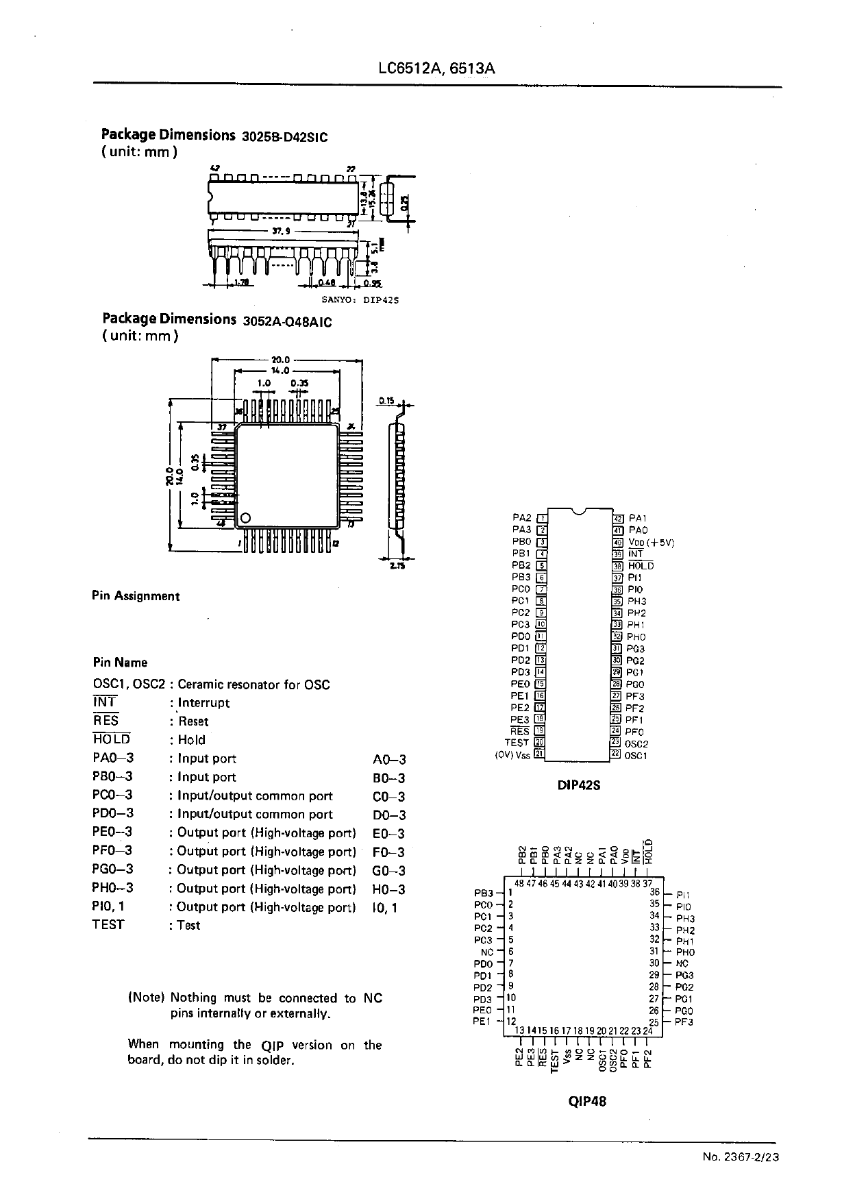
Pin Assignments
Pin Name
OSC1, OSC2 : Ceramic resonator for OSC
INT
: Interrupt
RES
: Reset
HOLD
: Hold
PAO-3
: Input port
A0–3
PBO-3
: Input port
B0–3
PCO-3
: Input/output common port
C0–3
PDO-3
: Input/output common port
D0–3
PEO-3
: Output port (High-voltage port) E0–3
PFO-3
: Output port (High-voltage port) F0–3
PGO-3
: Output port (High-voltage port) G0–3
PHO-3
: Output port (High-voltage port) H0–3
PI0, 1
: Output port (High-voltage port) I0, 1
TEST
: Test
DIP42S
(Note) Nothing must be connected to NC
pins internally or externally.
When mounting the QIP version on the
board, do not dip it in solder.
QIP48A
No.2367–2/24
Share Link: