LC75700T View Datasheet(PDF) - SANYO -> Panasonic
Part Name
Description
Manufacturer
LC75700T Datasheet PDF : 16 Pages
| |||
LC75700T
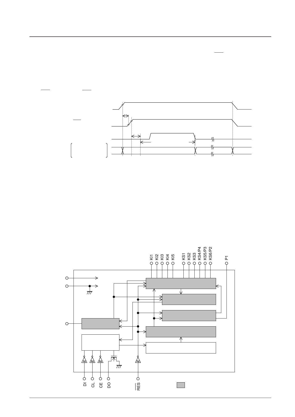
System Reset
When the power is first applied, the state of function is undefined, so it must be initialized by RES = “L”
1.Reset methods
This LSI stopprts the reset methods described below.
When a system reset is applied, key scanning is disabeled, the key data is reset, and the general-purpose output ports
are set to and held at the low level (VSS).
Set RES = “H” after the RES = “L” period. And key scanning become possible by the control data are transferred.
VDD
VDDmin
t1
RES
CE
KS1 to KS3
Output pins KS4/P4 to KS6/P2
P1
VIH1
VIL
t2
Control data transfer
"L"
VIL
Defined
Undefined
Notes: t1 ≥ 10 µs
t2 ≥ 10 µs
2.Internal block states during the reset period.
• CLOCK GENERATOR
Reset is applied and the basic clock is stopped. (The oscillator on the OSC pin is stopped.)
• KEY SCAN, KEY BUFFER
Reset is applied, the circuit is set to the initial state, and at the same time the key scan operation is disabled.
And all the key data is set to Low. Then, when the control data are transferred, the key scanning operation is enabled.
• GENERAL PORT
Reset is applied and the outputs of P1 to P4 are all set to the low level.
• CCB INTERFACE, SHIFT REGISTER, CONTROL REGISTER
When a reset is applied, The CONTROL REGISTER is forcibly initialized internally. Then, when control data are
transferred, the LSI operates according to the control data.
VDD
VSS
OSC
CLOCK
GENERATOR
CCB
INTERFACE
KEY SCAN
KEY BUFFER
GENERAL PORT
CONTROL REGISTER
SHIFT REGISTER
Blocks to which the reset applies.
No. 7632-12/16
Share Link: 