LC75864W View Datasheet(PDF) - SANYO -> Panasonic
Part Name
Description
Manufacturer
LC75864W Datasheet PDF : 26 Pages
| |||
LC75864E, 75864W
Voltage Detection Type Reset Circuit (VDET)
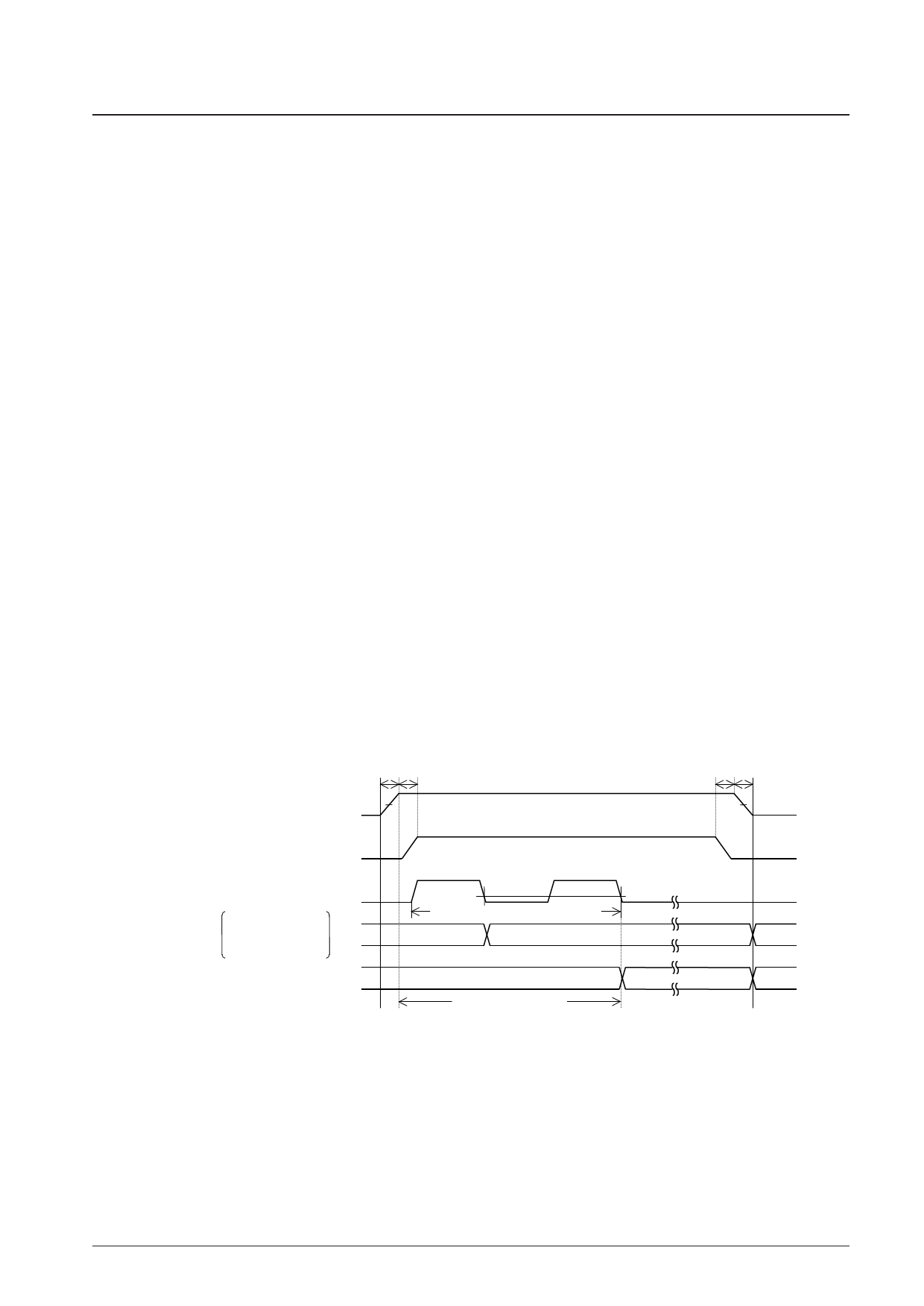
This circuit generates an output signal and resets the system when logic block power is first applied and when the
voltage drops, i.e., when the logic block power supply voltage is less than or equal to the power down detection voltage
VDET, which is 3.0 V, typical. To assure that this function operates reliably, a capacitor must be added to the logic
block power supply line so that the logic block power supply voltage VDD rise time when the logic block power is first
applied and the logic block power supply voltage VDD fall time when the voltage drops are both at least 1 ms.
(See Figure 3.)
Power Supply Sequence
The following sequences must be observed when power is turned on and off. (See Figure 3.)
• Power on: Logic block power supply (VDD) on → LCD driver block power supply (VLCD) on.
• Power off: LCD driver block power supply (VLCD) off → Logic block power supply (VDD) off.
However, if the logic and LCD driver block use a shared power supply, then the power supplies can be turned on and off
at the same time.
System Reset
The LC75864E/W supports the reset method described below. When a system reset is applied, display is turned off, key
scanning is stopped, and all the key data is reset to low. When the reset is cleared, display is turned on and key scanning
become possible.
1. Reset method
• Reset at power-on and power-down
If at least 1 ms is assured as the logic block supply voltage VDD rise time when logic block power is applied, a
system reset will be applied by the VDET output signal when the logic block supply voltage is brought up. If at
least 1 ms is assured as the logic block supply voltage VDD fall time when logic block power drops, a system reset
will be applied in the same manner by the VDET output signal when the supply voltage is lowered. Note that the
reset is cleared at the point when all the serial data (the display data D1 to D96 and the control data) has been
transferred, i.e., on the fall of the CE signal on the transfer of the last direction data, after all the direction data has
been transferred. (See Figure 3.)
VDD
VLCD
t1 t2
VDET
t3 t4
VDET
CE
D1 to D48
Internal data S0, S1, K0, K1
P0 to P2, SC, DR
Internal data (D49 to D96)
Display and control data transfer
Undefined
VIL
Defined
Undefined
System reset period
Defined
Note: • t1 ≥ 1 [ms] (Logic block power supply voltage VDD rise time)
• t2 ≥ 0
• t3 ≥ 0
• t4 ≥ 1 [ms] (Logic block power supply voltage VDD fall time)
Figure 3
Undefined
Undefined
No. 6860-17/26
Share Link: 