LC75864W View Datasheet(PDF) - SANYO -> Panasonic
Part Name
Description
Manufacturer
LC75864W Datasheet PDF : 26 Pages
| |||
LC75864E, 75864W
Control Data Functions
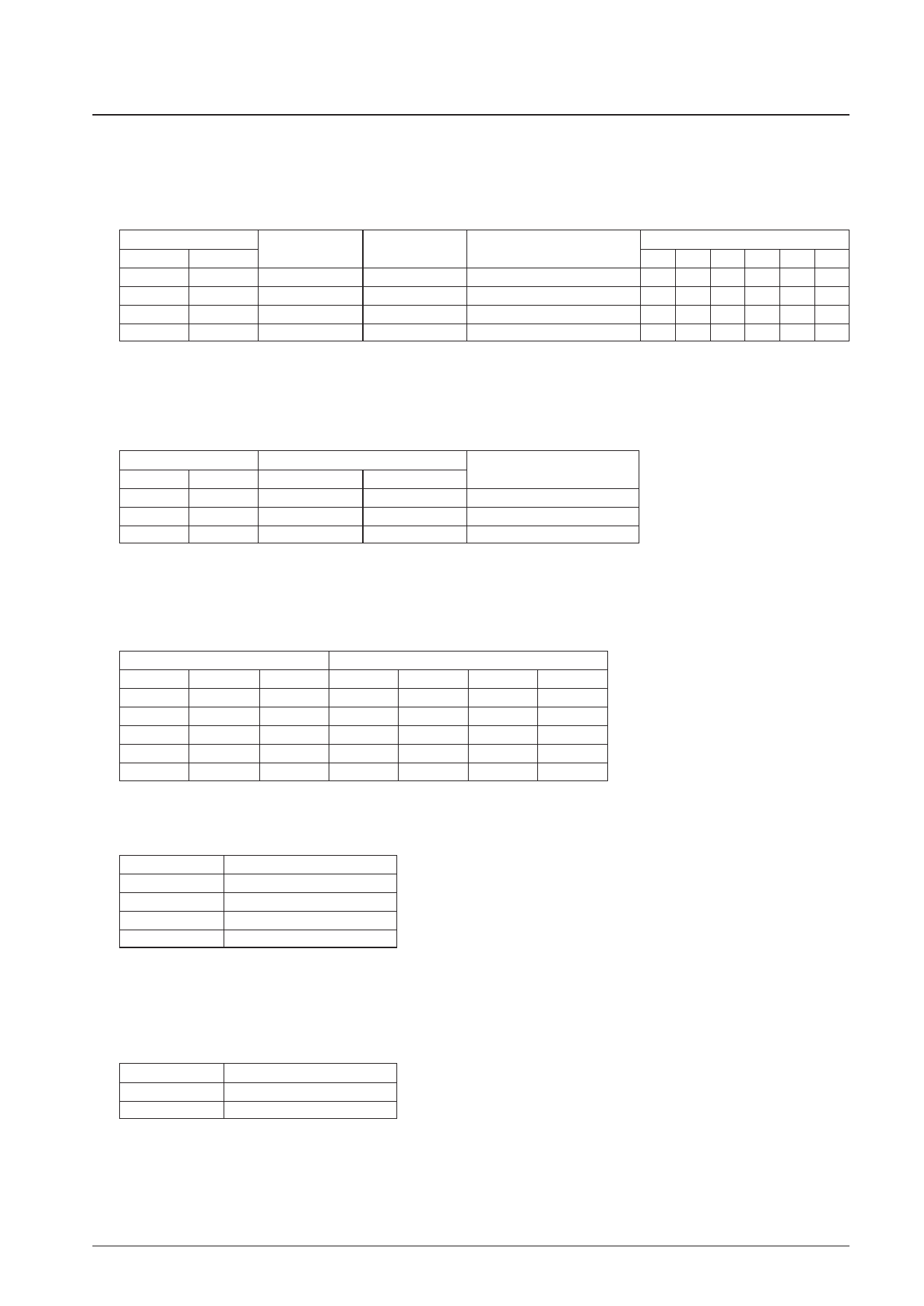
1. S0, S1: Sleep control data
These control data bits switch between normal mode and sleep mode and set the states of the KS1 to KS6 key scan
outputs during key scan standby.
Control data
S0
S1
0
0
0
1
1
0
1
1
Mode
Normal
Sleep
Sleep
Sleep
OSC oscillator
Operating
Stopped
Stopped
Stopped
Segment outputs
Common outputs
Operating
L
L
L
Output pin states during key scan standby
KS1 KS2 KS3 KS4 KS5 KS6
HHHH HH
L
L
L
L
L
H
L
L
L
L
HH
HHHH HH
Note: This assumes that the KS1/S23 and KS2/S24 output pins are selected for key scan output.
2. K0, K1: Key scan output/segment output selection data
These control data bits switch the functions of the KS1/S23 and KS2/S24 output pins between key scan output and
segment output.
Control data
K0
K1
0
0
0
1
1
!
!: don’t care
Output pin state
KS1/S23
KS2/S24
KS1
KS2
S23
KS2
S23
S24
Maximum number of input keys
30
25
20
Notes: KSn (n = 1 , 2): Key scan output
Sn (n = 23, 24): Segment output
3. P0 to P2: Segment output port/general-purpose output port selection data
These control data bits switch the functions of the S1/P1 to S4/P4 output pins between the segment output port and
the general-purpose output port.
Control data
P0
P1
P2
0
0
0
0
0
1
0
1
0
0
1
1
1
0
0
S1/P1
S1
P1
P1
P1
P1
Output pin state
S2/P2
S3/P3
S2
S3
S2
S3
P2
S3
P2
P3
P2
P3
S4/P4
S4
S4
S4
S4
P4
Notes: Sn (n = 1 to 4):
Segment output port
Pn (n = 1 to 4):
General-purpose output port
The table below lists the correspondence between the display data and the output pins when these pins are selected to
be general-purpose output ports.
Output pin
S1/P1
S2/P2
S3/P3
S4/P4
Corresponding display data
D1
D5
D9
D13
For example, if the S4/P4 output pin is selected to be a general-purpose output port, the S4/P4 output pin will output
a high level (VLCD) when the display data D13 is 1, and will output a low level(VSS) when D13 is 0.
4. SC: Segment on/off control data
This control data bit controls the on/off state of the segments.
SC
Display state
0
On
1
Off
However, note that when the segments are turned off by setting SC to 1, the segments are turned off by outputting
segment off waveforms from the segment output pins.
No. 6860-9/26
Share Link: 