LC83015 View Datasheet(PDF) - SANYO -> Panasonic
Part Name
Description
Manufacturer
LC83015 Datasheet PDF : 13 Pages
| |||
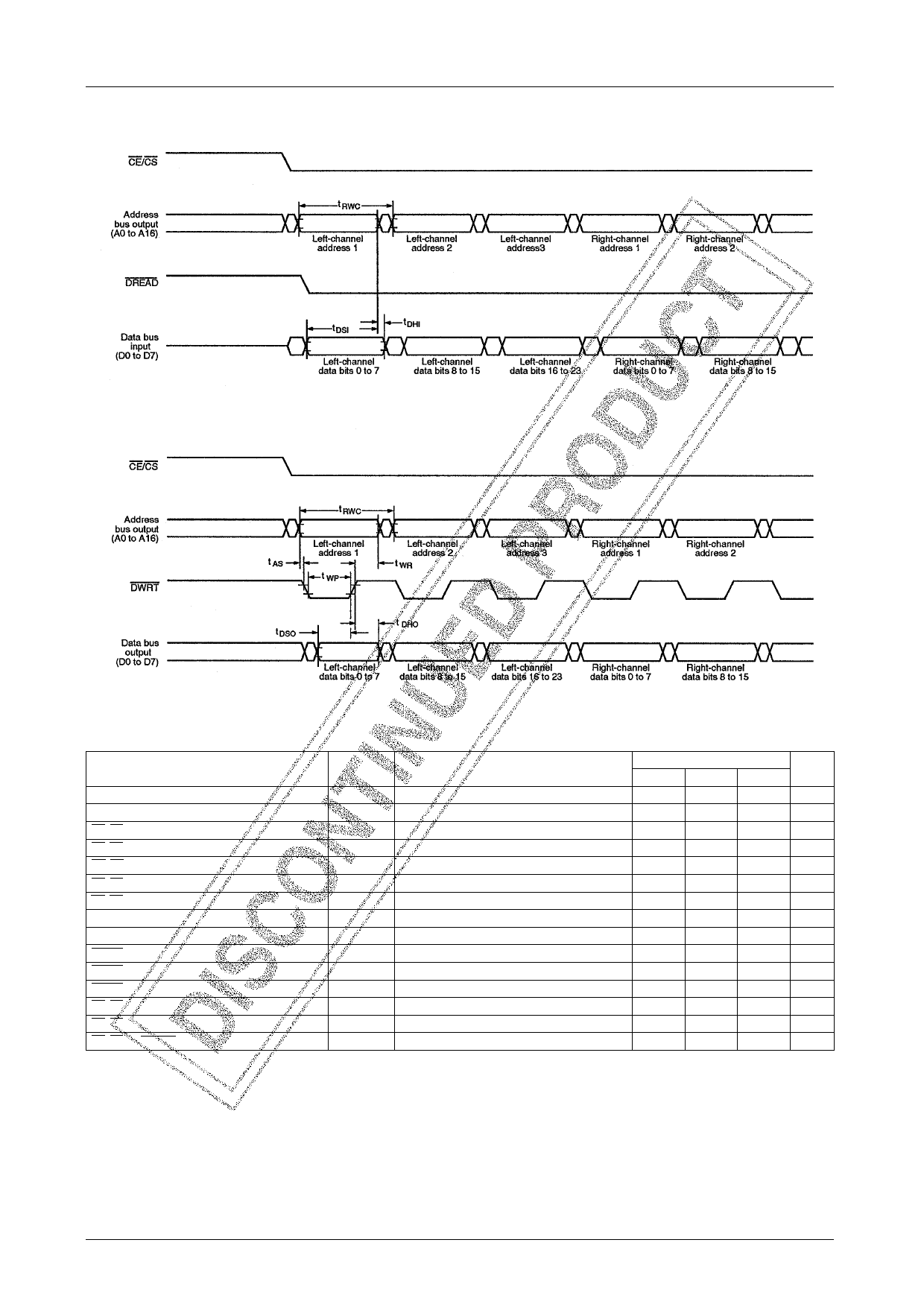
External SRAM Input Timing
LC83015E
External SRAM Output Timing
External Pseudo-SRAM Interface at Ta = –30 to +70˚C, VDD1 to VDD3 = 4.75 to 5.25 V, VSS1 to VSS4 = 0V
Parameter
Symbol
Conditions
Ratings
Unit
min
typ
max
Input data setup time
Input data hold time
CE/CS period
CE/CS pulsewidth
CE/CS pre-charge time
CE/CS address setup time
CE/CS address hold time
Write command hold time
Write command read time
DWRT pulsewidth
DWRT output data setup time
DWRT output data hold time
CE/CS output data setup time
CE/CS output data hold time
CE/CS to DREAD propagation delay
tDSI3
tDHI3
tC
tCES
tP
tASC
tAHC
tWCH
tCWL
tWP
tDSW
tDHW
tDSC
tDHC
tDER
10
ns
0
ns
160
ns
75
ns
75
ns
15
ns
100
ns
70
ns
70
ns
75
ns
50
ns
30
ns
50
ns
30
ns
0
30 ns
Note
Output timing values are measured with a load capacitance of 50 pF.
No.4013–8/13
Share Link: 