LC83015 View Datasheet(PDF) - SANYO -> Panasonic
Part Name
Description
Manufacturer
LC83015 Datasheet PDF : 13 Pages
| |||
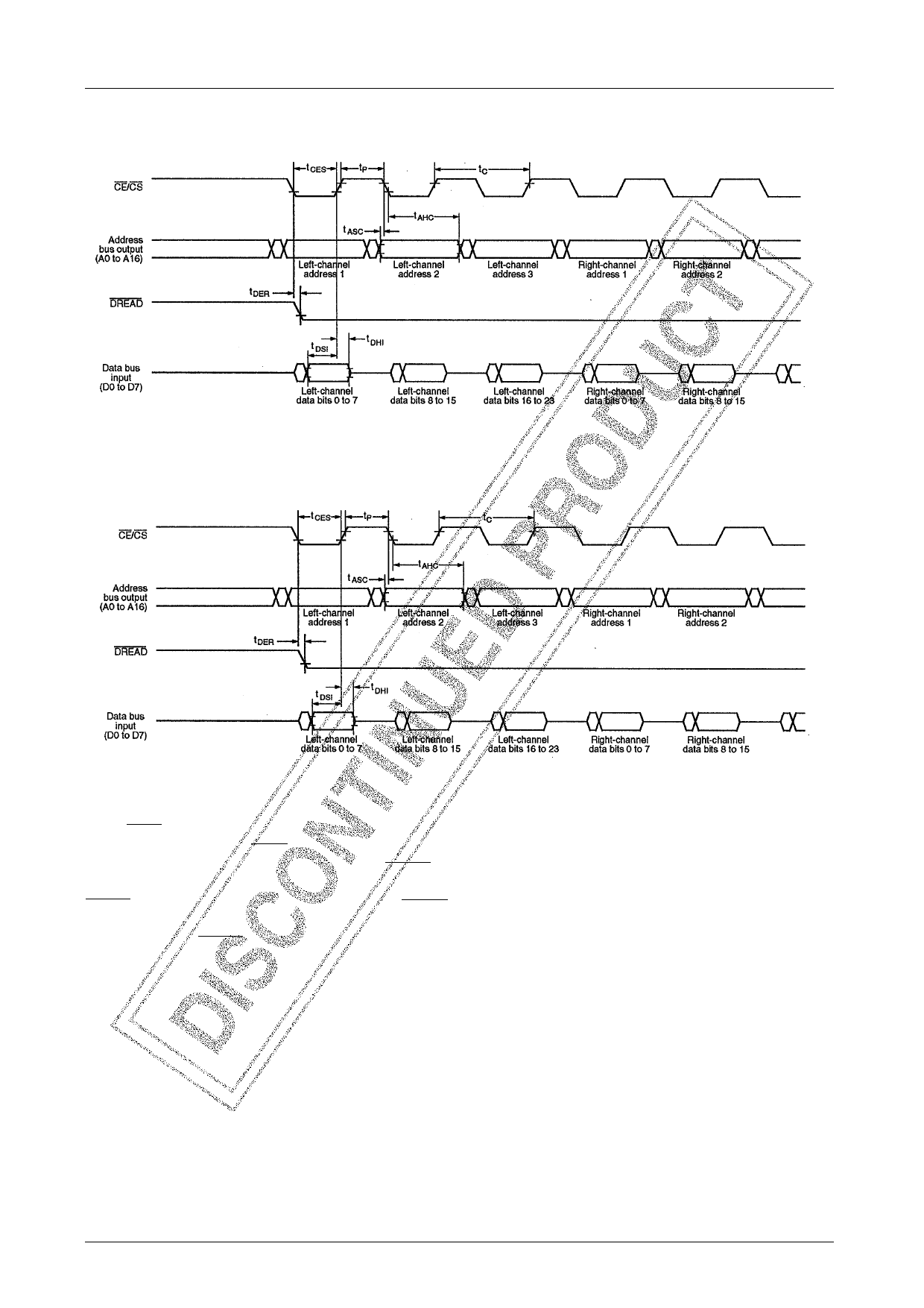
External Pseudo-SRAM Input Timing
LC83015E
External Pseudo-SRAM Output Timing
Design Notes
When SELC is LOW, the LC83015E system clock is gener-
ated from FS384I. When SELC is HIGH, it is generated
from the free-running oscillator, OSC1. When SACK1 is
LOW, FS384O output is 1/3 of FS128O output. When
SACK1 is HIGH, it is 1/4 of FS128O output. When SACK2
is LOW, the output clock is generated from FS384I, LRCKI
and BCK1. When SACK2 is HIGH, it is generated from the
free-running oscillator, OSC1.
When the LC83015E is used with one DRAM unit, only
D0 to D3 of the data bus are used. When the LC83015E is
used with two DRAM units, SRAM or pseudo-SRAM, D0
to D7 are used.
The typical supply current, IDD, is measured with SANYO
Standard Theatre Mode in operation under the input/output
conditions shown in figure 1.
No.4013–9/13
Share Link: 