PEMT1 View Datasheet(PDF) - Philips Electronics
Part Name
Description
Manufacturer
PEMT1 Datasheet PDF : 8 Pages
| |||
Philips Semiconductors
PNP general purpose double transistor
Product specification
PEMT1
FEATURES
• 300 mW total power dissipation
• Very small 1.6 × 1.2 mm ultra thin package
• Self alignment during soldering due to straight leads
• Replaces two SC-75/SC-89 packaged transistors on
same PCB area
• Reduced required PCB area
• Reduced pick and place costs.
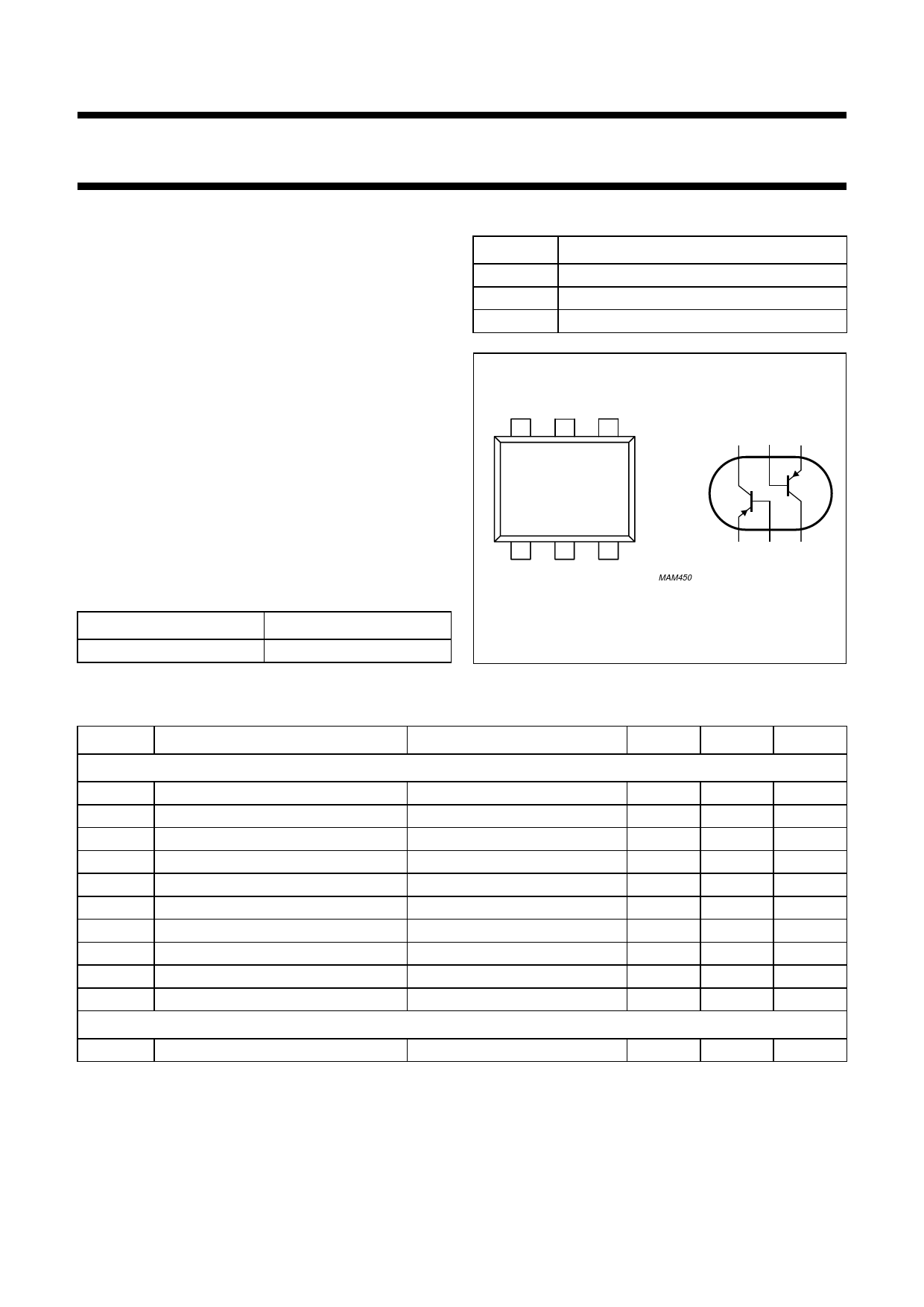
PINNING
PIN
1, 4
2, 5
6, 3
emitter
base
collector
DESCRIPTION
TR1; TR2
TR1; TR2
TR1; TR2
APPLICATIONS
• General purpose switching and amplification.
DESCRIPTION
PNP transistor pair in a SOT666 plastic package.
NPN complement: PEMX1.
MARKING
TYPE NUMBER
PEMT1
MARKING CODE
FF
6
5
4
65 4
TR2
TR1
1
2
3
Top view
MAM450
123
Fig.1 Simplified outline (SOT666) and symbol.
LIMITING VALUES
In accordance with the Absolute Maximum Rating System (IEC 60134).
SYMBOL
PARAMETER
CONDITIONS
Per transistor
VCBO
VCEO
VEBO
IC
ICM
IBM
Ptot
Tstg
Tj
Tamb
collector-base voltage
collector-emitter voltage
emitter-base voltage
collector current (DC)
peak collector current
peak base current
total power dissipation
storage temperature
junction temperature
operating ambient temperature
Per device
Ptot
total power dissipation
open emitter
open base
open collector
Tamb ≤ 25 °C; note 1
Tamb ≤ 25 °C; note 1
Note
1. Transistor mounted on an FR4 printed-circuit board.
MIN.
MAX.
UNIT
−
−50
V
−
−40
V
−
−5
V
−
−100
mA
−
−200
mA
−
−200
mA
−
200
mW
−65
+150
°C
−
150
°C
−65
+150
°C
−
300
mW
2001 Nov 07
2
Share Link: 