LS6501LP(2001) View Datasheet(PDF) - LSI Corporation
Part Name
Description
Manufacturer
LS6501LP Datasheet PDF : 8 Pages
| |||
PARAMETER
SYMBOL
OUTPUT DRIVE CURRENT:
Triac (AC MODE)
IO
Relay (DC MODE)
IO
TRIAC OUTPUT TIMING:
Pulse Width
Delay from zero crossover
TTPW
TOD
Delay difference between
zero crossovers
TODD
AC INPUT IMPEDANCE
ZAC
LED OUTPUT:
Sink Current
ILS
Pulse Width
TLPW
DUAL PULSE MODE:
Time between pulse-pairs
TR
for motion recognition
MIN
-40
-10
20
1.00
-
270
-
.75
-
TYP
-
-
30
1.2
-
-
-
1
-
MAX
-
-
45
1.32
150
-
8
1.25
5.125
UNIT CONDITIONS
mA
With 3V Triac Gate Drive
mA
With 1V Max. across the
LS6501LP.
µs
VDD = 8V, f = 60Hz and
ms
2.7V P-P AC input
µs
f = 60Hz
kΩ
-
mA
VDD = 8V, Vo = .5V Max.
sec
f = 60Hz.
sec
-
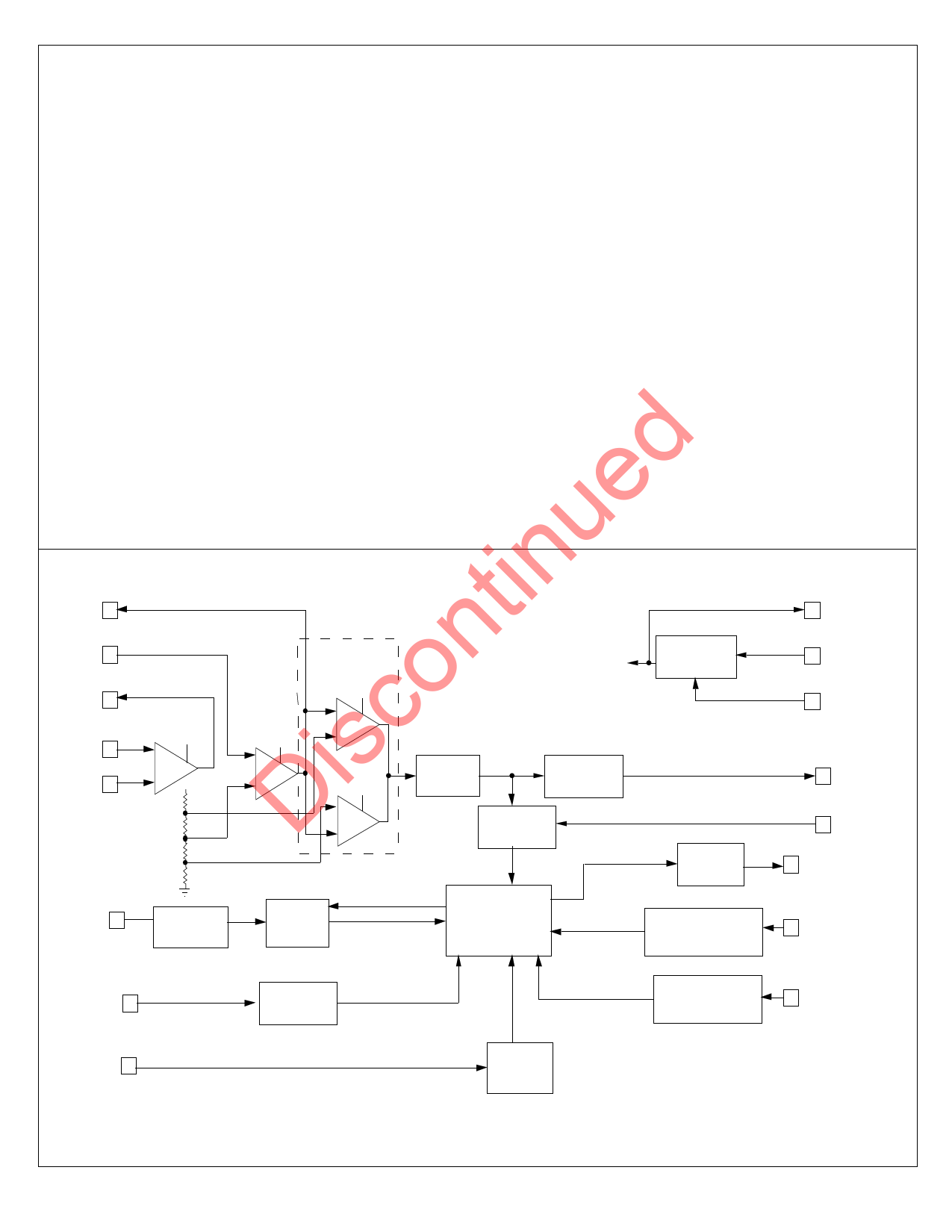
DIFF AMP 2 3
OUTPUT
DIFF AMP 2
INPUT (-)
2
DIFF AMP 1 1
OUTPUT
DIFF AMP 1
INPUT (-)
16
DIFF AMP 1 15
INPUT (+)
VREG
-
AMP
+
VREG
TIMER
CONTROL 13
INPUT
A/D
CONVERTER
WINDOW
COMPARATOR
V REG
-
AMP
+
V REG
-
COMP
+
V REG
-
COMP
+
OUTPUT
DURATION
TIMER
VREG
5 VOLT
REGULATOR
14
5V REGULATOR
OUTPUT
8 VDD
6 VSS
DIGITAL
FILTER
1 SECOND
PULSE GEN
PULSE
SELECT
LOGIC
CONTROL
LOGIC
OUTPUT
BUFFER
9 LED OUTPUT
10
PULSE MODE
SELECT INPUT
7 TRIAC/RELAY OUTPUT
ZERO CROSS-OVER
DETECT
5 AC INPUT
INHIBIT INPUT 11
DEAD TIME
SELECT INPUT
12
6501LP-070601-4
INHIBIT
COMPARATOR
DEAD
TIME
TIMER
OSCILLATOR
4 OSCILLATOR INPUT
FIGURE 2. LS6501LP BLOCK DIAGRAM
Share Link: 