LT1764EQ-1.8(RevA) View Datasheet(PDF) - Linear Technology
Part Name
Description
Manufacturer
LT1764EQ-1.8 Datasheet PDF : 16 Pages
| |||
LT1764 Series
APPLICATIONS INFORMATION
Thermal Considerations
The power handling capability of the device is limited by
the maximum rated junction temperature (125°C). The
power dissipated by the device is made up of two compo-
nents:
1. Output current multiplied by the input/output voltage
differential: (IOUT)(VIN – VOUT), and
2. GND pin current multiplied by the input voltage:
(IGND)(VIN).
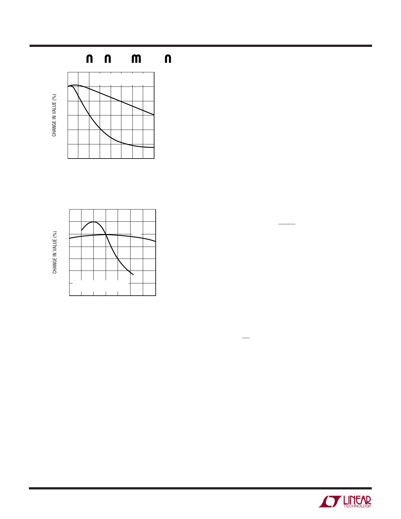
The GND pin current can be found using the GND Pin
Current curves in the Typical Performance Characteris-
tics. Power dissipation will be equal to the sum of the two
components listed above.
The LT1764 series regulators have internal thermal limit-
ing designed to protect the device during overload condi-
tions. For continuous normal conditions, the maximum
junction temperature rating of 125°C must not be
exceeded. It is important to give careful consideration to
all sources of thermal resistance from junction to ambient.
Additional heat sources mounted nearby must also be
considered.
For surface mount devices, heat sinking is accomplished
by using the heat spreading capabilities of the PC board
and its copper traces. Surface mount heatsinks and plated
through-holes can also be used to spread the heat gener-
ated by power devices.
The following table lists thermal resistance for several
different board sizes and copper areas. All measurements
were taken in still air on 1/16" FR-4 board with one ounce
copper.
Table 1. Q Package, 5-Lead DD
COPPER AREA
TOPSIDE* BACKSIDE BOARD AREA
2500mm2
1000mm2
125mm2
2500mm2
2500mm2
2500mm2
2500mm2
2500mm2
2500mm2
*Device is mounted on topside.
THERMAL RESISTANCE
(JUNCTION-TO-AMBIENT)
23°C/ W
25°C/ W
33°C/ W
T Package, 5-Lead TO-220
Thermal Resistance (Junction-to-Case) = 2.5°C/W
Calculating Junction Temperature
Example: Given an output voltage of 3.3V, an input voltage
range of 4V to 6V, an output current range of 0mA to
500mA and a maximum ambient temperature of 50°C,
what will the maximum junction temperature be?
The power dissipated by the device will be equal to:
IOUT(MAX)(VIN(MAX) – VOUT) + IGND(VIN(MAX))
where,
IOUT(MAX) = 500mA
VIN(MAX) = 6V
IGND at (IOUT = 500mA, VIN = 6V) = 10mA
So,
P = 500mA(6V – 3.3V) + 10mA(6V) = 1.41W
Using a DD package, the thermal resistance will be in the
range of 23°C/W to 33°C/W depending on the copper
area. So the junction temperature rise above ambient will
be approximately equal to:
1.41W(28°C/W) = 39.5°C
The maximum junction temperature will then be equal to
the maximum junction temperature rise above ambient
plus the maximum ambient temperature or:
TJMAX = 50°C + 39.5°C = 89.5°C
Protection Features
The LT1764 regulators incorporate several protection
features which make them ideal for use in battery-powered
circuits. In addition to the normal protection features
associated with monolithic regulators, such as current
limiting and thermal limiting, the devices are protected
against reverse input voltages, reverse output voltages
and reverse voltages from output to input.
Current limit protection and thermal overload protection
are intended to protect the device against current overload
conditions at the output of the device. For normal opera-
tion, the junction temperature should not exceed 125°C.
The input of the device will withstand reverse voltages of
20V. Current flow into the device will be limited to less than
1mA and no negative voltage will appear at the output. The
1764fa
12
Share Link: 