LT1782HS6 View Datasheet(PDF) - Linear Technology
Part Name
Description
Manufacturer
LT1782HS6 Datasheet PDF : 16 Pages
| |||
LT1782
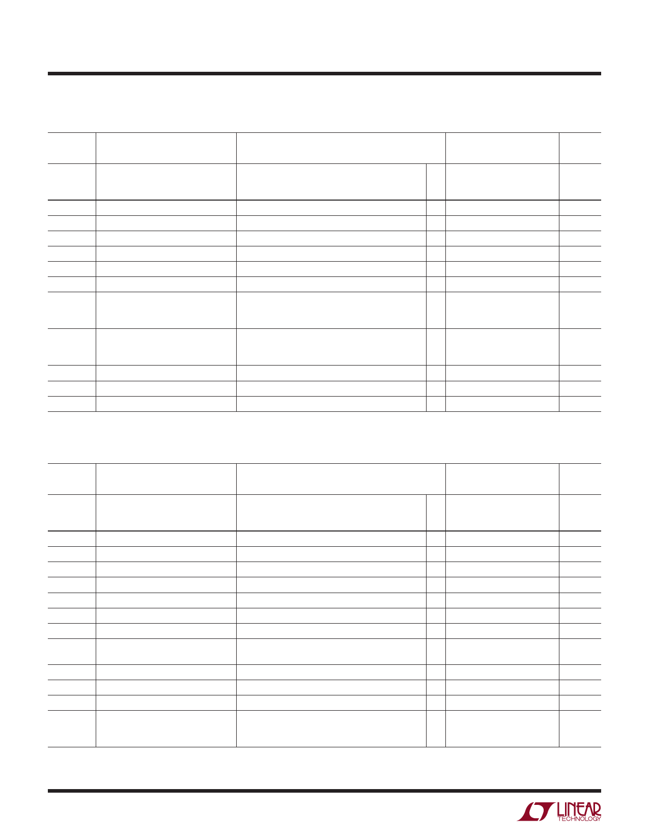
ELECTRICAL CHARACTERISTICS The l denotes the specifications which apply over the full operating
temperature range, otherwise specifications are at TA = 25°C. VS = 3V, 0V; VS = 5V, 0V, VCM = VOUT = half supply, for the 6-lead part
VPIN5 = 0V, pulse power tested unless otherwise specified.
LT1782C/LT1782I
SYMBOL PARAMETER
CONDITIONS
MIN
TYP MAX
UNITS
ISHDN
Shutdown Pin Current
VPIN5 = 0.3V, No Load (Note 10)
VPIN5 = 2V, No Load (Note 10)
VPIN5 = 5V, No Load (Note 10)
l
0.5
nA
l
2
8
µA
l
5
µA
Shutdown Output Leakage Current VPIN5 = 2V, No Load (Note 10)
l
0.05
1
µA
Maximum Shutdown Pin Current
VPIN5 = 18V, No Load (Note 10)
l
10
30
µA
VL
Shutdown Pin Input Low Voltage (Note 10)
l
0.3
V
VH
Shutdown Pin Input High Voltage (Note 10)
l
2
V
tON
Turn-On Time
VPIN5 = 5V to 0V, RL = 10k (Note 10)
100
µs
tOFF
Turn-Off Time
VPIN5 = 0V to 5V, RL = 10k (Note 10)
6
µs
GBW
Gain Bandwidth Product
(Note 5)
f = 5kHz
0°C ≤ TA ≤ 70°C
–40°C ≤ TA ≤ 85°C
110
200
kHz
l 100
kHz
l 90
kHz
SR
Slew Rate
(Note 5)
AV = –1, RL = ∞
0°C ≤ TA ≤ 70°C
–40°C ≤ TA ≤ 85°C
0.035 0.07
V/µs
l 0.031
V/µs
l 0.028
V/µs
tS
Settling Time
VS = 5V, ∆VOUT = 2V to 0.1%, AV = –1
45
µs
THD
Distortion
VS = 3V, VO = 2VP-P, AV = 1, RL = 10k, f = 1kHz
0.003
%
FPBW
Full-Power Bandwidth (Note 9)
VOUT = 2VP-P
11
kHz
The l denotes the specifications which apply over the full operating temperature range, otherwise specifications
VS = ±5V, VCM = 0V, VOUT = 0V, for the 6-lead part VPIN5 = V–, pulse power tested unless otherwise specified.
are
at
TA
=
25°C.
SYMBOL
VOS
∆VOS/∆T
IOS
IB
en
in
RIN
CIN
CMRR
AVOL
PARAMETER
Input Offset Voltage
Input Offset Voltage Drift (Note 7)
Input Offset Current
Input Bias Current
Input Bias Current Drift
Input Noise Voltage
Input Noise Voltage Density
Input Noise Current Density
Input Resistance
Input Capacitance
Input Voltage Range
Common Mode Rejection Ratio
Large-Signal Voltage Gain
CONDITIONS
TA = 25°C
0°C ≤ TA ≤ 70°C
–40°C ≤ TA ≤ 85°C
0.1Hz to 10Hz
f = 1kHz
f = 1kHz
Differential
Common Mode, VCM = –5V to 13V
VCM = –5V to 13V
VO = ±4V, RL = 10k
0°C ≤ TA ≤ 70°C
–40°C ≤ TA ≤ 85°C
LT1782C/LT1782I
MIN
TYP MAX
500 900
l
1050
l
1200
l
2
5
l
0.7
2
l
8
15
l
0.01
1
50
0.05
l 3.4
6.5
l 1.5
3
5
l –5
13
l 68
80
55
150
l 40
l 30
UNITS
µV
µV
µV
µV/°C
nA
nA
nA/°C
µVP-P
nV/√Hz
pA/√Hz
MΩ
MΩ
pF
V
dB
V/mV
V/mV
V/mV
1782fc
4
Share Link: 