LT1764A View Datasheet(PDF) - Linear Technology
Part Name
Description
Manufacturer
LT1764A Datasheet PDF : 20 Pages
| |||

LT1764A Series
ELECTRICAL CHARACTERISTICS
The ● denotes specifications which apply over the full operating temperature range, otherwise specifications are TA = 25°C. (Note 2)
PARAMETER
CONDITIONS
Current Limit
VIN = 7V, VOUT = 0V
E Grade: LT1764A; LT1764A-1.5;
VIN = 2.7V, ∆VOUT = – 0.1V
MP Grade: LT1764A
VIN = 2.8V, ∆VOUT = – 0.1V
Input Reverse Leakage Current VIN = – 20V, VOUT = 0V
Reverse Output Current (Note 10) LT1764A-1.5 VOUT = 1.5V, VIN < 1.5V
LT1764A-1.8 VOUT = 1.8V, VIN < 1.8V
LT1764A-2.5 VOUT = 2.5V, VIN < 2.5V
LT1764A-3.3 VOUT = 3.3V, VIN < 3.3V
LT1764A (Note 3) VOUT = 1.21V, VIN < 1.21V
MIN TYP
4
● 3.1
MAX UNITS
A
A
● 3.1
A
●
1
mA
600
1200
µA
600
1200
µA
600
1200
µA
600
1200
µA
300
600
µA
Note 1: Stresses beyond those listed under Absolute Maximum Ratings
may cause permanent damage to the device. Exposure to any Absolute
Maximum Rating condition for extended periods may affect device
reliability and lifetime.
Note 2: The LT1764A regulators are tested and specified under pulse load
conditions such that TJ ≈ TA. The LT1764A (E grade) is 100% tested at
TA = 25°C; performance at – 40°C and 125°C is assured by design,
characterization and correlation with statistical process controls. The
LT1764A (MP grade) is 100% tested and guaranteed over the –55°C to
125°C temperature range.
Note 3: The LT1764A (adjustable version) is tested and specified for these
conditions with the ADJ pin connected to the OUT pin.
Note 4. Operating conditions are limited by maximum junction temperature.
The regulated output voltage specification will not apply for all possible
combinations of input voltage and output current. When operating at max-
imum input voltage, the output current range must be limited. When operat-
ing at maximum output current, the input voltage range must be limited.
Note 5: To satisfy requirements for minimum input voltage, the LT1764A
(adjustable version) is tested and specified for these conditions with an
external resistor divider (two 4.12k resistors) for an output voltage of
2.42V. The external resistor divider will add a 300µA DC load on the output.
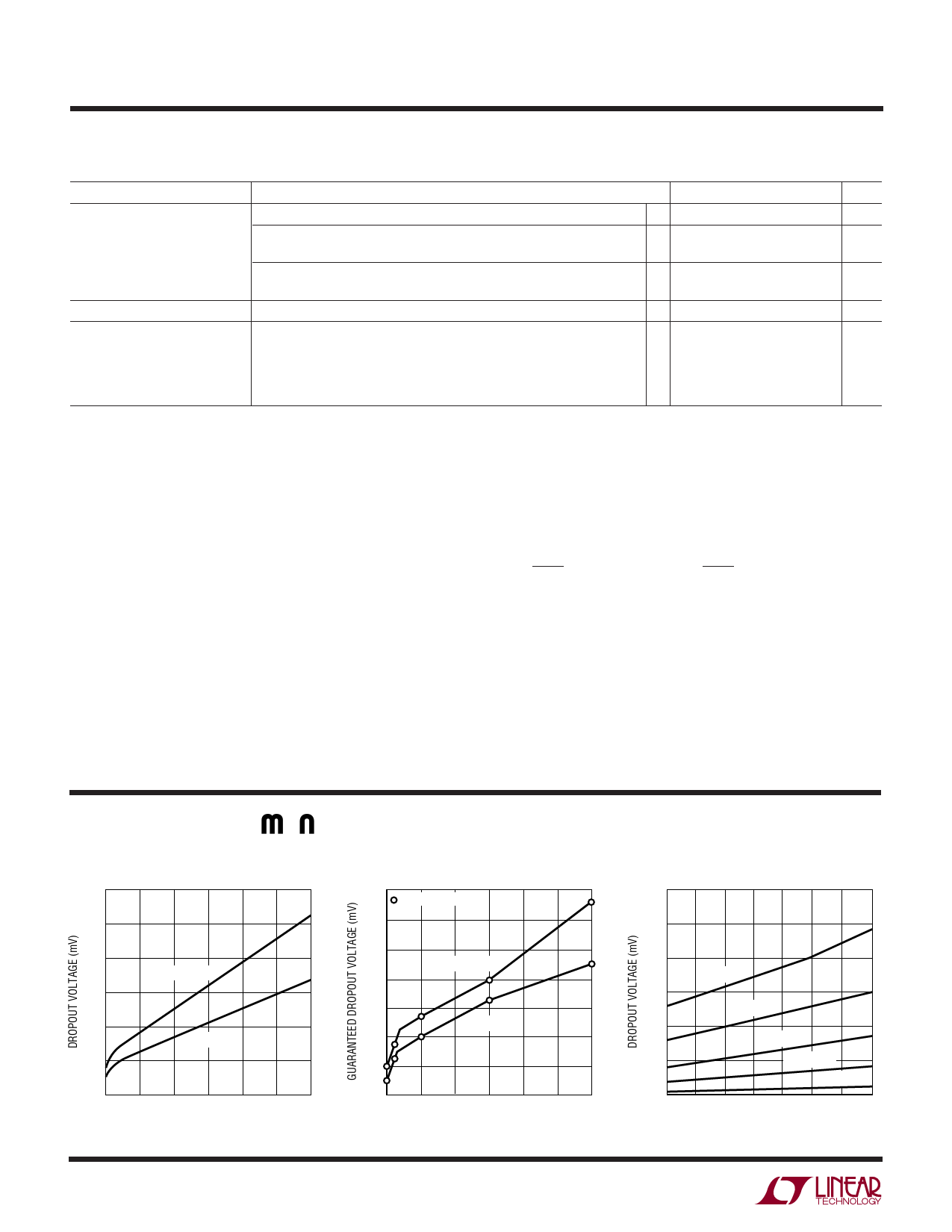
Note 6: Dropout voltage is the minimum input to output voltage differential
needed to maintain regulation at a specified output current. In dropout, the
output voltage will be equal to: VIN – VDROPOUT.
Note 7: GND pin current is tested with VIN = VOUT(NOMINAL) + 1V or VIN =
2.7V (E grade) or VIN = 2.8V (MP grade), whichever is greater, and a current
source load. The GND pin current will decrease at higher input voltages.
Note 8: ADJ pin bias current flows into the ADJ pin.
Note 9: SHDN pin current flows into the SHDN pin.
Note 10: Reverse output current is tested with the IN pin grounded and the
OUT pin forced to the rated output voltage. This current flows into the OUT
pin and out the GND pin.
Note 11. For the LT1764A, LT1764A-1.5 and LT1764A-1.8 dropout voltage
will be limited by the minimum input voltage specification under some
output voltage/load conditions.
Note 12. All combinations of absolute maximum input voltage and
absolute maximum output voltage cannot be achieved. The absolute
maximum differential from input to output is ±20V. For example, with
VIN = 20V, VOUT cannot be pulled below ground.
TYPICAL PERFOR A CE CHARACTERISTICS
Typical Dropout Voltage
600
500
400
TJ = 125°C
300
200
TJ = 25°C
100
0
0 0.5 1.0 1.5 2.0 2.5 3.0
OUTPUT CURRENT (A)
1764 G01
Guaranteed Dropout Voltage
700
= TEST POINTS
600
500
TJ ≤ 125°C
400
300
TJ ≤ 25°C
200
100
0
0 0.5 1.0 1.5 2.0 2.5 3.0
OUTPUT CURRENT (A)
1764 G02
4
Dropout Voltage
600
500
400
IL = 3A
300
IL = 1.5A
200
IL = 0.5A
100
0
–50 –25
IL = 100mA
IL = 1mA
0 25 50 75
TEMPERATURE (°C)
100 125
1764 G03
1764afb