LT1933HS6(RevD) View Datasheet(PDF) - Linear Technology
Part Name
Description
Manufacturer
LT1933HS6
(Rev.:RevD)
(Rev.:RevD)
Linear Technology

LT1933HS6 Datasheet PDF : 20 Pages
| |||
LT1933
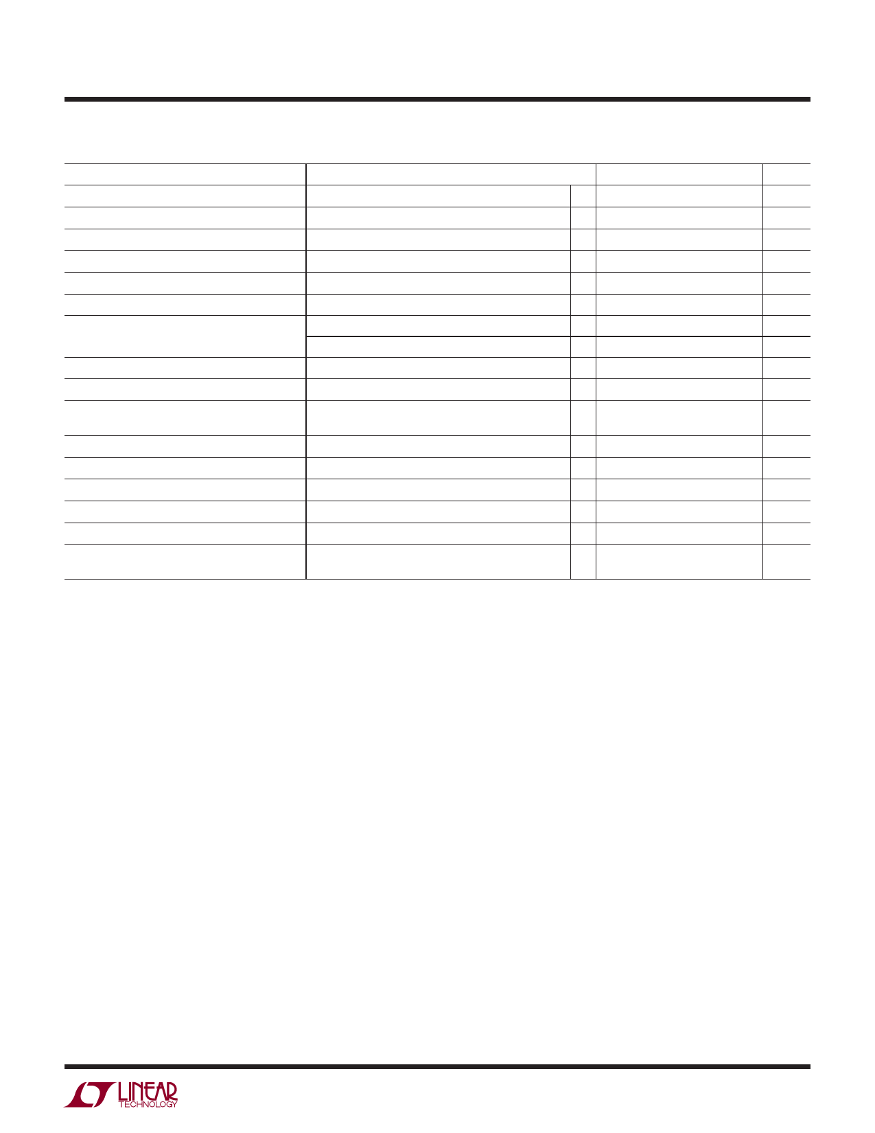
ELECTRICAL CHARACTERISTICS The l denotes the specifications which apply over the full operating
temperature range, otherwise specifications are at TA = 25°C. VIN = 12V, VBOOST = 17V, unless otherwise noted. (Note 2)
PARAMETER
CONDITIONS
MIN TYP
MAX
UNITS
Undervoltage Lockout
3.35
3.6
V
Feedback Voltage
l 1.225 1.245 1.265
V
FB Pin Bias Current
Quiescent Current
VFB = Measured VREF + 10mV (Note 4)
Not Switching
l
40
120
nA
1.6
2.5
mA
Quiescent Current in Shutdown
VSHDN = 0V
0.01
2
μA
Reference Line Regulation
Switching Frequency
Maximum Duty Cycle
VIN = 5V to 36V
VFB = 1.1V
VFB = 0V
0.01
%/V
400
500
600
kHz
55
kHz
l 88
94
%
Switch Current Limit
(Note 3)
0.75 1.05
A
Switch VCESAT
Switch Leakage Current
ISW = 400mA, S6 Package
ISW = 400mA, DCB6 Package
370
500
mV
370
mV
2
μA
Minimum Boost Voltage Above Switch
BOOST Pin Current
SHDN Input Voltage High
SHDN Input Voltage Low
SHDN Bias Current
ISW = 400mA
ISW = 400mA
VSHDN = 2.3V (Note 5)
VSHDN = 0V
1.9
2.3
V
18
25
mA
2.3
V
0.3
V
34
50
μA
0.01
0.1
μA
Note 1: Stresses beyond those listed under Absolute Maximum Ratings
may cause permanent damage to the device. Exposure to any Absolute
Maximum Rating condition for extended periods may affect device
reliability and lifetime.
Note 2: The LT1933E is guaranteed to meet performance specifications
from 0°C to 70°C. Specifications over the –40°C to 85°C operating
temperature range are assured by design, characterization and correlation
with statistical process controls. The LT1933I specifications are
guaranteed over the –40°C to 125°C temperature range. The LT1933H
specifications are guaranteed over the –40°C to 150°C temperature range.
Note 3: Current limit guaranteed by design and/or correlation to static test.
Slope compensation reduces current limit at higher duty cycle.
Note 4: Current flows out of pin.
Note 5: Current flows into pin.
1933fd
3
Share Link: