LT3150 View Datasheet(PDF) - Linear Technology
Part Name
Description
Manufacturer
LT3150
Linear Technology

LT3150 Datasheet PDF : 20 Pages
| |||
LT3150
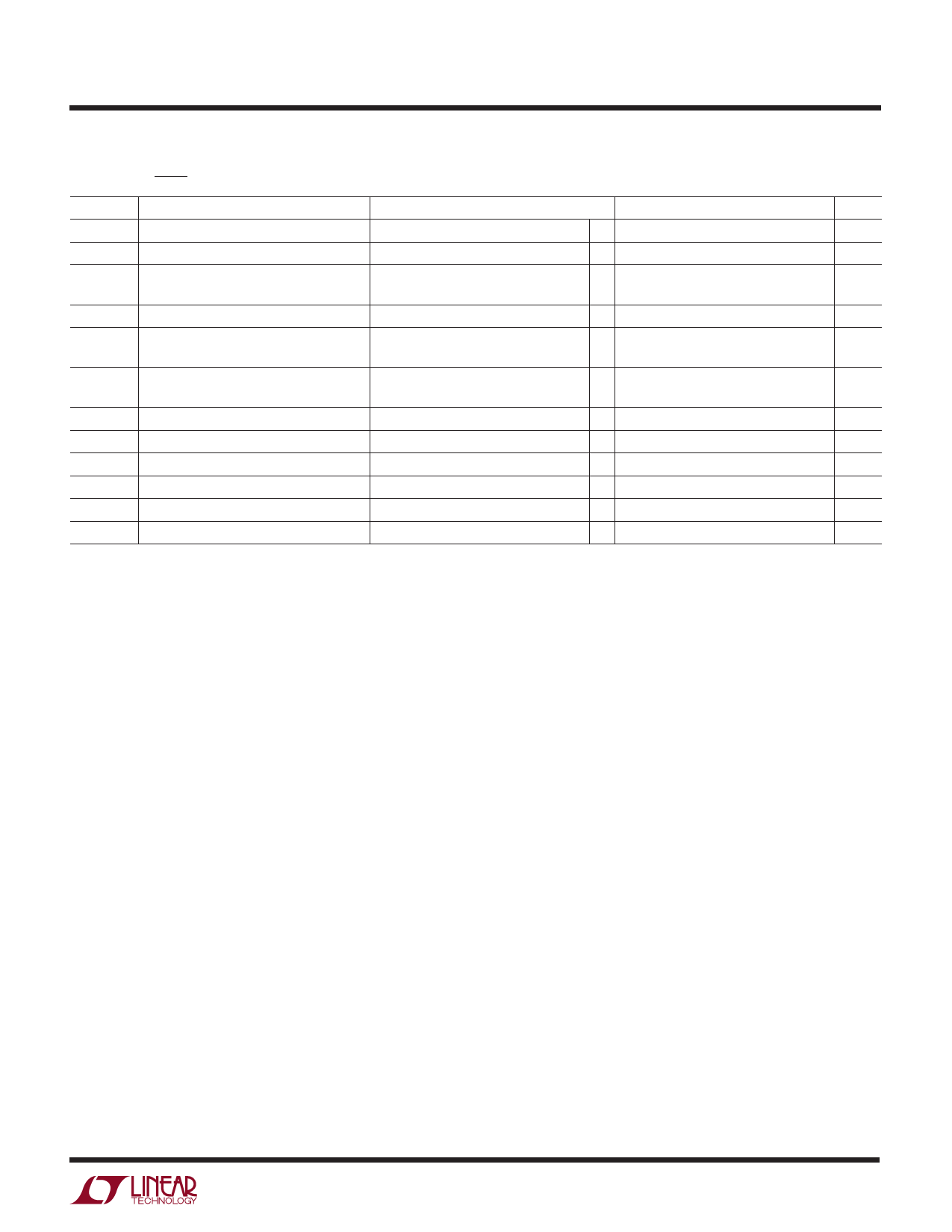
ELECTRICAL CHARACTERISTICS
The q denotes specifications which apply over the full operating temperature range, otherwise specifications are at TA = 25°C.
VIN1 = 1.5V, VSHDN1 = VIN1, VIN2 = 12V, GATE = 6V, IPOS = INEG = 5V, VSHDN2 = 0.75V unless otherwise noted.
SYMBOL PARAMETER
CONDITIONS
MIN
TYP
MAX
UNITS
AVOL
Large-Signal Voltage Gain
VOL
GATE Output Swing Low (Note 4)
VOH
GATE Output Swing High
VGATE = 3V to 10V
IGATE = 0mA
IGATE = 0mA
q
69
84
dB
q
2.5
3
V
q VIN2 – 1.6 VIN2 – 1
V
IPOS + INEG Supply Current
Current Limit Threshold Voltage
Current Limit Threshold Voltage
Line Regulation
SHDN2 Sink Current
SHDN2 Source Current
SHDN2 Low Clamp Voltage
SHDN2 High Clamp Voltage
SHDN2 Threshold Voltage
SHDN2 Threshold Hysteresis
3V ≤ IPOS ≤ 20V
3V ≤ IPOS ≤ 20V
Current Flows Into Pin
Current Flows Out of Pin
q
0.3
0.625
1
mA
42
50
58
mV
q
37
50
63
mV
q
– 0.20 – 0.50
%/V
q
2.5
5.0
8.0
µA
q
–8
– 15
– 23
µA
q
0.1
0.25
V
q
1.50
1.85
2.20
V
q
1.18
1.21
1.240
V
q
50
100
150
mV
Note 1: Absolute Maximum Ratings are those values beyond which the life
of the device may be impaired.
Note 2: TJ is calculated from the ambient temperature TA and power
dissipation PD according to the following formula:
TJ = TA + (PD • 130°C/W)
Note 3: Switch current limit is guaranteed by design and/or correlation to
static test.
Note 4: The VGS(th) of the external MOSFET must be greater than
3V – VOUT.
3150f
3
Share Link: