LT3460 View Datasheet(PDF) - Linear Technology
Part Name
Description
Manufacturer
LT3460 Datasheet PDF : 12 Pages
| |||
LT3460/LT3460-1
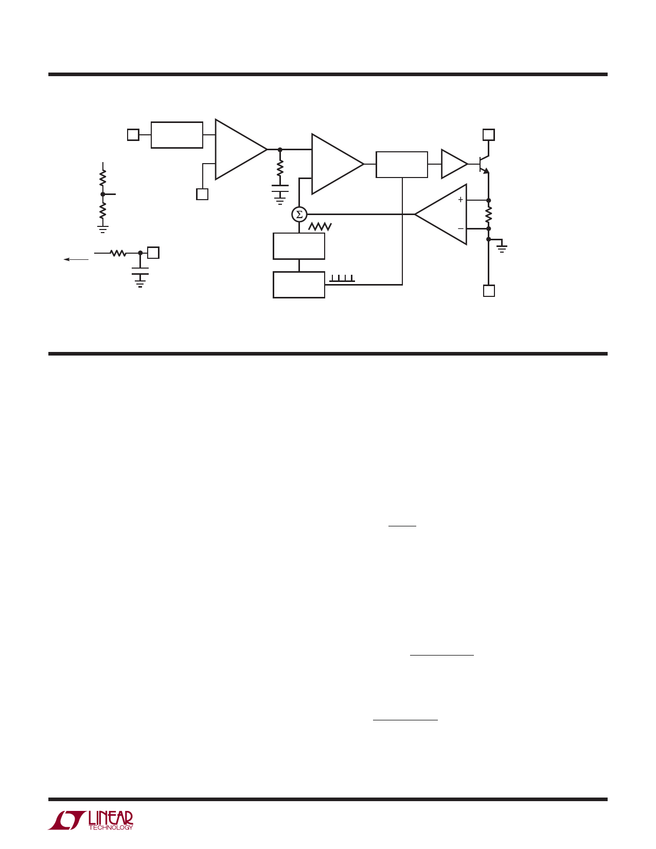
BLOCK DIAGRAM
VIN
VOUT
1.255V
REFERENCE
R1 (EXTERNAL)
FB
R2 (EXTERNAL)
+
A1
–
FB
COMPARATOR
DRIVER
–
RC
A2
+
CC
R
Q
S
SW
Q1
0.1Ω
RS (EXTERNAL)
SHUTDOWN
SHDN
CS (EXTERNAL)
RS, CS OPTIONAL SOFT-START COMPONENTS
RAMP
GENERATOR
1.3MHz
OSCILLATOR
Figure 1. Block Diagram, LT3460
GND
3460 BD
OPERATION
The LT3460/LT3460-1 uses a constant frequency, current
mode control scheme to provide excellent line and load
regulation. Operation can be best understood by referring to
the block diagram in Figure 1. At the start of each oscillator
cycle, the SR latch is set, which turns on the power switch
Q1. A voltage proportional to the switch current is added
to a stabilizing ramp and the resulting sum is fed into the
positive terminal of the PWM comparator A2. When this
voltage exceeds the level at the negative input of A2, the
SR latch is reset turning off the power switch. The level at
the negative input of A2 is set by the error amplifier A1, and
is simply an amplified version of the difference between
the feedback voltage and the reference voltage of 1.255V.
In this manner, the error amplifier sets the correct peak
current level to keep the output in regulation. If the error
amplifier’s output increases, more current is delivered to
the output; if it decreases, less current is delivered.
Feedback Loop Compensation
The LT3460/LT3460-1 has an internal feedback compensa-
tion network as shown in Figure 1 (RC and CC). However,
because the small signal characteristics of a boost converter
change with operation conditions, the internal compensa-
tion network cannot satisfy all applications. A properly
designed external feed forward capacitor from VOUT to
FB (CF in Figure 2) will correct the loop compensation for
most applications.
The LT3460/LT3460-1 uses peak current mode control.
The current feedback makes the inductor very similar
to a current source in the medium frequency range. The
power stage transfer function in the medium frequency
range can be approximated as:
GP(s)
=
K1
s • C2
,
where C2 is the output capacitance, and K1 is a constant
based on the operating point of the converter. In continuous
current mode, K1 increases as the duty cycle decreases.
The internal compensation network RC, CC can be ap-
proximated as follows in medium frequency range:
GC(s)
=
K2
•
s
•
RC • CC
s • CC
+
1
The zero
fZ
=
2
•
•
1
RC
•
CC
is about 70kHz.
3460fb
5
Share Link: 