LT3579FE(RevA) View Datasheet(PDF) - Linear Technology
Part Name
Description
Manufacturer
LT3579FE Datasheet PDF : 42 Pages
| |||
LT3579/LT3579-1
APPLICATIONS INFORMATION
SEPIC CONVERTER COMPONENT SELECTION
– COUPLED OR UN-COUPLED INDUCTORS
VPWR
9V TO 16V
VIN
3.3V
TO 5V
CVIN
4.7µF
L1
6.8µH
CPWR
4.7µF
C1
4.7µF
SW1 SW2
VIN
FB
SHDN
GATE
100k
LT3579
D1
60V, 3A
L2
6.8µH
RFB
130k
VOUT
12V
1.6A (VPWR >9V)
1.9A (VPWR >12V)
COUT
10µF
×3
FAULT CLKOUT
RT
RT SYNC GND
86.6k
VC
SS
CSS
0.22µF
CF
47pF
RC
9.53k
CC
2.2nF
35791 F07
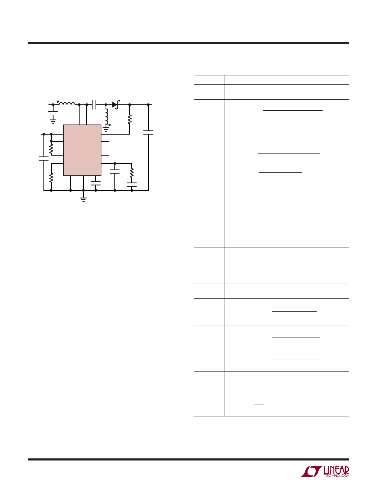
Figure 7. SEPIC Converter – The Component Values Given Are
Typical Values for a 1MHz, 9V–16V to 12V SEPIC Topology Using
Coupled Inductors
The LT3579 can also be configured as a SEPIC as in
Figure 7. This topology allows for positive output voltages
that are lower, equal, or higher than the input voltage. Output
disconnect is inherently built into the SEPIC topology,
meaning no DC path exists between the input and output
due to capacitor C1. This implies that a PMOS controlled
by the GATE pin is not required in the power path.
Table 2 is a step-by-step set of equations to calculate
component values for the LT3579 when operating as a
SEPIC converter using coupled inductors. Input parameters
are input and output voltage, and switching frequency
(VIN, VOUT and fOSC respectively). Refer to the Appendix
for further information on the design equations presented
in Table 2.
Variable Definitions:
VIN = Input Voltage
VOUT = Output Voltage
DC = Power Switch Duty Cycle
fOSC = Switching Frequency
IOUT = Maximum Output Current
IRIPPLE = Inductor Ripple Current
Table 2. SEPIC Design Equations
Step 1:
Inputs
PARAMETERS/EQUATIONS
Pick VIN, VOUT, and fOSC to calculate equations below.
Step 2: DC
DC ≅
VIN
+
VOUT + 0.5V
VOUT + 0.5V – 0.27V
Step 3: L
Step 4:
IRIPPLE
( ) LTYP =
VIN – 0.27V • DC
fOSC • 1.8A
(1)
LMIN
=
( VIN
– 0.27V) • (2 • DC –
4A • fOSC • (1 – DC)
1)
(2)
( ) LMAX =
VIN – 0.27V • DC
fOSC • 0.5A
(3)
• Solve equations 1, 2, and 3 for a range of L values.
• The minimum of the L value range is the higher of
LTYP and LMIN.
• The maximum of the L value range is LMAX.
• L = L1 = L2 for coupled inductors.
• L = L1||L2 for uncoupled inductors.
( ) IRIPPLE =
VIN – 0.27V • DC
fOSC • L
Step 5: IOUT
( ) IOUT
=
6A
–
IRIPPLE
2
•
1 – DC
Step 6: D1
Step 7: C1
VR > VIN + VOUT ; IAVG > IOUT
4.7µF (typical) ; VRATING > VIN
Step 8: COUT
COUT
=
fOSC
IOUT • DC
• 0.005 •VOUT
Step 9: CPWR
CPWR
=
8•
IRIPPLE
fOSC • 0.005 •
VIN
Step 10: CVIN
Step 11: RFB
CVIN
=
40
•
6A • DC
fOSC • 0.005
•
VIN
RFB
=
VOUT – 1.215V
83.3µA
Step 12: RT
RT
=
87.6
fOSC
– 1; fOSC
in MHz
and RT
in kΩ
Note: The maximum design target for peak switch current is 6A and
is used in this table. The final values for COUT, CPWR, and CVIN may
deviate from the above equations in order to obtain desired load
transient performance for a particular application.
35791fa
14
For more information www.linear.com/LT3579
Share Link: 