LT3971IDD View Datasheet(PDF) - Linear Technology
Part Name
Description
Manufacturer
LT3971IDD Datasheet PDF : 28 Pages
| |||
LT3971/LT3971-3.3/LT3971-5
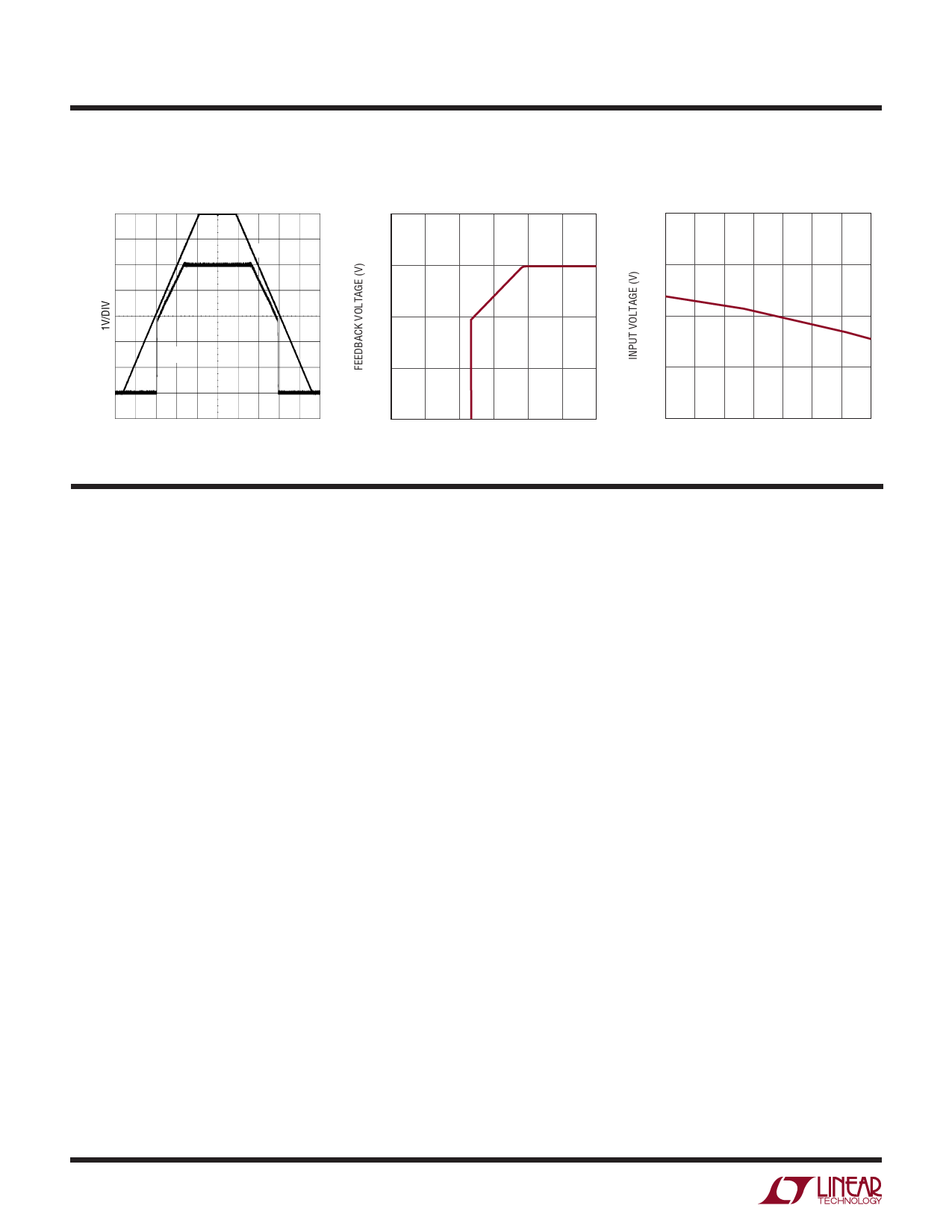
TYPICAL PERFORMANCE CHARACTERISTICS TA = 25В°C, unless otherwise noted.
5V Start-Up and Dropout
VIN
Feedback Regulation Voltage
1.6
1.2
Minimum Input Voltage to Switch
5
4
0.8
3
VOUT
0.4
2
800kHz
10О© LOAD
0.5s/DIV
3971 G34
0
2 2.5 3 3.5 4 4.5 5
INPUT VOLTAGE (V)
3971 G35
1
вҖ“55 вҖ“25
5 35 65 95
TEMPERATURE (В°C)
125 155
3971 G36
PIN FUNCTIONS (DFN, MSE10/MSE16)
BD (Pin 1/Pin 1): This pin connects to the anode of the
boost diode. The BD pin is normally connected to the output.
BOOST (Pin 2/Pin 3): This pin is used to provide a drive
voltage, higher than the input voltage, to the internal bipolar
NPN power switch.
SW (Pin 3/Pin 5): The SW pin is the output of an internal
power switch. Connect this pin to the inductor, catch diode,
and boost capacitor.
VIN (Pin 4/Pin 7): The VIN pin supplies current to the
LT3971вҖҷs internal circuitry and to the internal power switch.
This pin must be locally bypassed.
EN (Pin 5/Pin 8): The part is in shutdown when this pin
is low and active when this pin is high. The hysteretic
threshold voltage is 1.005V going up and 0.975V going
down. The EN threshold is only accurate when VIN is above
4.3V. If VIN is lower than 4.2V, ground EN to place the part
in shutdown. Tie to VIN if shutdown feature is not used.
FB (Pin 6, LT3971 Only/Pins 9, 10): The LT3971 regulates
the FB pin to 1.19V. Connect the feedback resistor divider
tap to this pin. Also, connect a phase lead capacitor between
FB and VOUT. Typically this capacitor is 10pF.
VOUT (Pin 6, LT3971-3.3 and LT3971-5 Only): The
LT3971вҖ‘3.3 and LT3971-5 regulate the VOUT pin to 3.3V and
5V respectively. This pin connects to the internal 10MО©
feedback divider that programs the fixed output voltage.
8
SS (Pin 7/Pin 12): A capacitor is tied between SS and
ground to slowly ramp up the peak current limit of the
LT3971 on start-up. The soft-start capacitor is only actively
discharged when EN is low. The SS pin is released when
the EN pin goes high. Float this pin to disable soft-start.
For applications with input voltages above 25V, add a 100k
resistor in series with the soft-start capacitor.
RT (Pin 8/Pin 13): A resistor is tied between RT and ground
to set the switching frequency.
PG (Pin 9/Pin 14): The PG pin is the open-drain output of
an internal comparator. PGOOD remains low until the FB
pin is within 9% of the final regulation voltage. PGOOD is
valid when the LT3971 is enabled and VIN is above 4.3V.
SYNC (Pin 10/Pin 15): This is the external clock synchro-
nization input. Ground this pin for low ripple Burst Mode
operation at low output loads. Tie to a clock source for
synchronization, which will include pulse-skipping at low
output loads. When in pulse-skipping mode, quiescent
current increases to 1.5mA.
GND (Exposed Pad Pin 11/Pin 16, Exposed Pad Pin 17):
Ground. The exposed pad must be soldered to PCB.
NC (None/Pins 2, 4, 6, 11): No Connect. These pins
are not connected to internal circuitry. Float these pins
to achieve FMEA fault tolerance. (See Fault Tolerance of
MS16E Package section.)
3971fd
Share Link: 