LT6703IDC-3TRMPBF View Datasheet(PDF) - Linear Technology
Part Name
Description
Manufacturer
LT6703IDC-3TRMPBF Datasheet PDF : 14 Pages
| |||
LT6703-2/LT6703-3
LT6703HV-2/LT6703HV-3
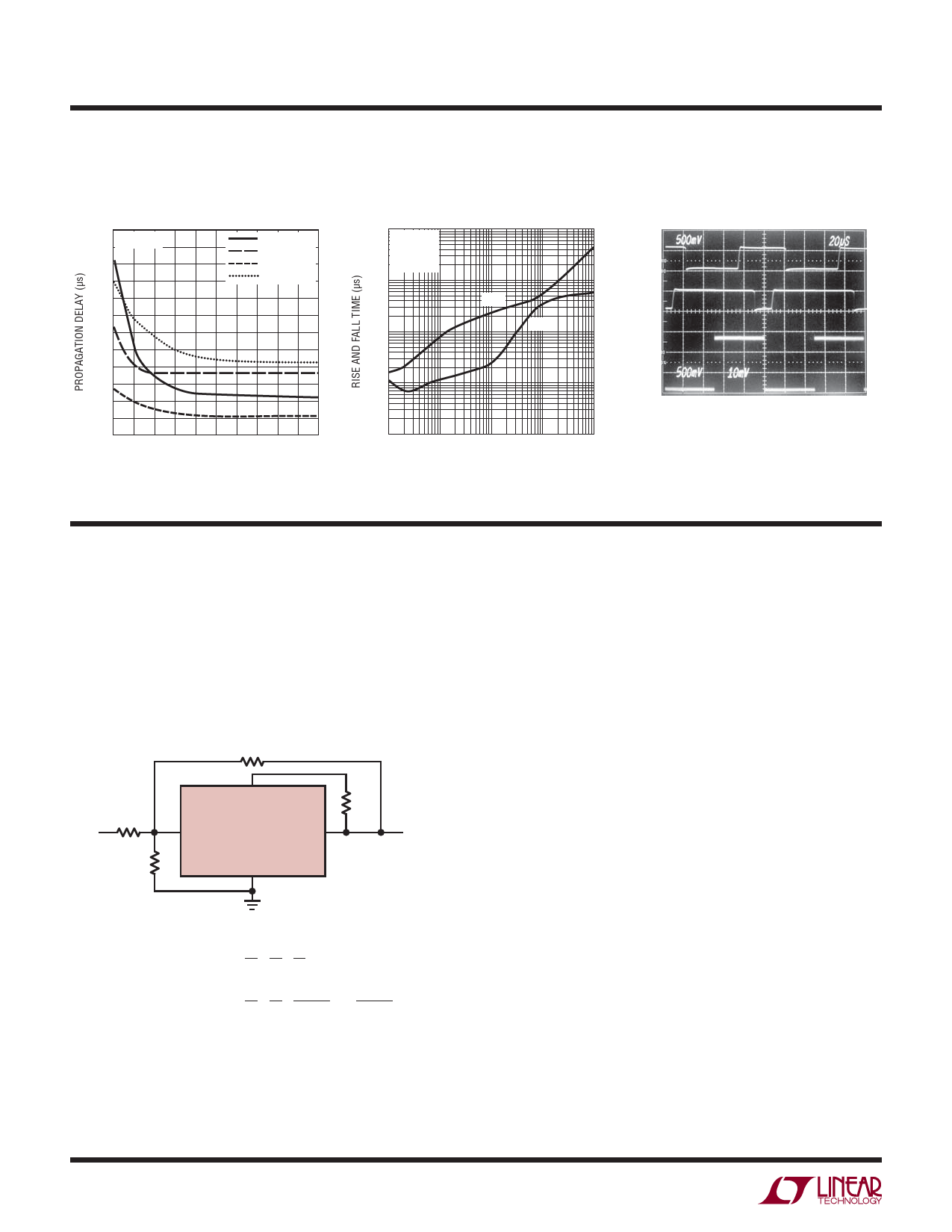
TYPICAL PERFORMANCE CHARACTERISTICS
Propagation Delay
vs Input Overdrive
60
TA = 25°C
50
40
LH NONINV
HL NONINV
LH INV
HL INV
30
20
10
0
0
20
40
60
80 100
INPUT OVERDRIVE (mV)
670323 G25
Rise and Fall Times
vs Output Pull-Up Resistor
100
VS = 5V
CL = 20pF
TA = 25°C
10
RISE
1
FALL
0.1
Noninverting and Inverting
Comparator Propagation Delay
VO(NINV)
5V/DIV
DC
VO(INV)
5V/DIV
DC
VIN
10mV/DIV
AC
0.01
0.1
1
10
100
1000
OUTPUT PULL-UP RESISTOR (kΩ)
670323 G26
VS = 5V
20μs/DIV
670323 G27
TA = 25°C
RLOAD = 10k CONNECTED TO VS
VIN(OVERDRIVE) = 10mV OVER THE INPUT
VOLTAGE THRESHOLDS
APPLICATIONS INFORMATION
The LT6703-2/LT6703-3/LT6703HV-2/LT6703HV-3 devices
are micropower comparators with a built-in 400mV refer-
ence. Features include wide supply voltage range (1.4V to
18V), Over-The-Top input and output range, 2% accurate
rising input threshold voltage and 6.5mV typical built-in
hysteresis.
R3
R1
VIN
+IN
R2
VS
R4
LT6703-3
OUT
GND
670323 F01
VOUT
THRESHOLD EQUATIONS:
VIN (L TO H) = (400mV) • (R1) •
1 11
++
R1 R2 R3
VIN (H TO L) = (393mV) • (R1) • 1 + 1 + 1
R1 R2 R3 + R4
– VS • R1
R3 + R4
Figure 1. Additional Hysteresis Circuit
Internal Reference
Each comparator has one input available externally. The two
versions of the part differ by the polarity of the available
input (i.e., inverting or noninverting). The other comparator
input is connected internally to the 400mV reference. The
rising input threshold voltage of the comparator is designed
to be equal to that of the reference (i.e., ≈400mV). The
reference voltage is established with respect to the device
GND connection.
Hysteresis
Each comparator has built-in 6.5mV (typical) of hysteresis
to simplify designs, to insure stable operation in the pres-
ence of noise at the inputs, and to reject supply rail noise
that might be induced by state change load transients. The
hysteresis is designed such that the falling input threshold
voltage is nominally 393.5mV. External positive feedback
circuitry can be employed to increase effective hysteresis
if desired, but such circuitry will provide an apparent effect
on both the rising and falling input thresholds (the actual
internal thresholds remain unaffected).
10
670323fd
Share Link: 