LTC1346 View Datasheet(PDF) - Linear Technology
Part Name
Description
Manufacturer
LTC1346 Datasheet PDF : 12 Pages
| |||
LTC1346A
AC ELECTRICAL CHARACTERISTICS VCC = 5V ±5%, VEE = –5V ±5% (Note 2)
SYMBOL PARAMETER
CONDITIONS
MIN
ICC
VCC Supply Current
IEE
VEE Supply Current
tr, tf
tPLH
tPHL
tSKEW
tPLH
tPHL
tSKEW
Transmitter Rise or Fall Time
Transmitter Input to Output
Transmitter Input to Output
Transmitter Output to Output
Receiver Input to Output
Receiver Input to Output
Differential Receiver Skew, tPLH – tPHL
VOS = 0V, S0 = Low, S1 = S2 = High (Figure 1) q
No Load, S0 = Low, S1 = S2 = High
q
Shutdown, S0 = VCC, S1 = S2 = 0V
q
VOS = 0V, S0 = Low, S1 = S2 = High (Figure 1) q
No Load, S0 = Low, S1 = S2 = High
q
Shutdown, S0 = VCC, S1 = S2 = 0V
q
VOS = 0V (Figures 1, 3)
q
VOS = 0V (Figures 1, 3)
q
VOS = 0V (Figures 1, 3)
q
VOS = 0V (Figures 1, 3)
VOS = 0V (Figures 1, 4)
q
VOS = 0V (Figures 1, 4)
q
VOS = 0V (Figures 1, 4)
tZL
Receiver Enable to Output Low (Active Mode) CL = 15pF, SW1 Closed (Figures 2, 5)
q
Receiver Enable to Output Low
(from Shutdown, Note 3)
CL = 15pF, SW1 Closed (Figures 2, 5)
tZH
Receiver Enable to Output High (Active Mode) CL = 15pF, SW2 Closed (Figures 2, 5)
q
Receiver Enable to Output High
(from Shutdown, Note 3)
CL = 15pF, SW2 Closed (Figures 2, 5)
tLZ
Receiver Disable from Low
tHZ
Receiver Disable from High
CL = 15pF, SW1 Closed (Figures 2, 5)
q
CL = 15pF, SW2 Closed (Figures 2, 5)
q
TYP MAX UNITS
40
50
mA
6
9
mA
0.1
100
µA
– 40 – 50
mA
–6
–9
mA
– 0.1 – 100
µA
7
40
ns
25
70
ns
30
70
ns
5
ns
50
100
ns
55
100
ns
5
ns
40
70
ns
2
µs
35
70
ns
2
µs
30
70
ns
35
70
ns
The q denotes specifications which apply over the full operating
temperature range.
Note 1: The Absolute Maximum Ratings are those values beyond which
the life of a device may be impaired.
Note 2: All currents into device pins are positive; all currents out of device
pins are termed negative. All voltages are referenced to device ground
unless otherwise specified.
Note 3: Receiver enable to output valid high or low from shutdown is
typically 2µs.
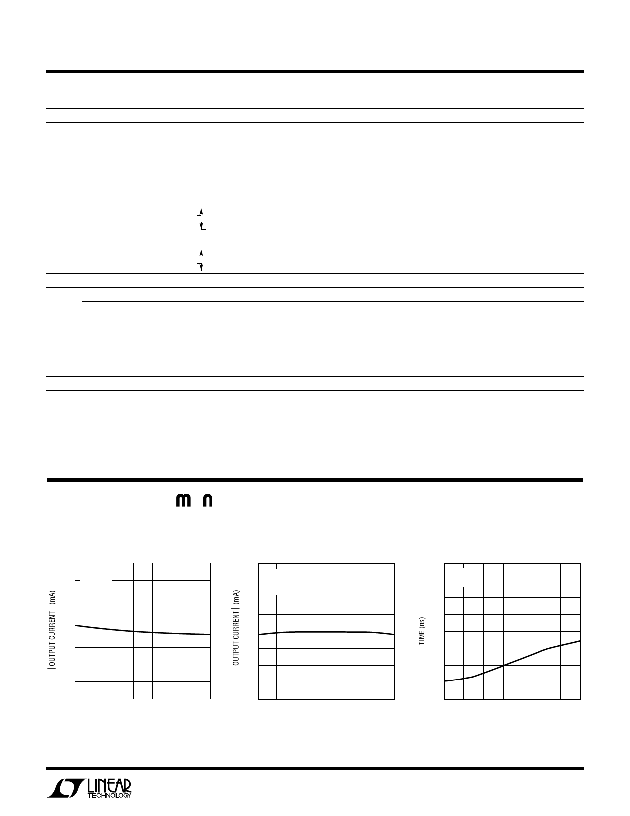
TYPICAL PERFORMANCE CHARACTERISTICS
Transmitter Output Current
vs Temperature
13
VCC = 5V
VEE = –5V
12
11
10
9
–50 –25
0 25 50 75
TEMPERATURE (˚C)
100 125
1346A G01
Transmitter Output Current
vs Output Voltage
13
TA = 25°C
VCC = 5V
VEE = –5V
12
11
10
9
–2.0 –1.5 –1.0 –0.5 0 0.5 1.0 1.5 2.0
OUTPUT VOLTAGE (V)
1346A G02
Transmitter Output Skew
vs Temperature
20
VCC = 5V
VEE = –5V
15
10
5
0
–50 –25
0 25 50 75
TEMPERATURE (˚C)
100 125
1346A G03
3
Share Link: 