LTC1346 View Datasheet(PDF) - Linear Technology
Part Name
Description
Manufacturer
LTC1346 Datasheet PDF : 12 Pages
| |||
LTC1346A
APPLICATIONS INFORMATION
CHIP
VCC
BOUNDARY
11mA
Y
50Ω 125Ω
T
50Ω
Z
11mA
VEE
LTC1346A • F07
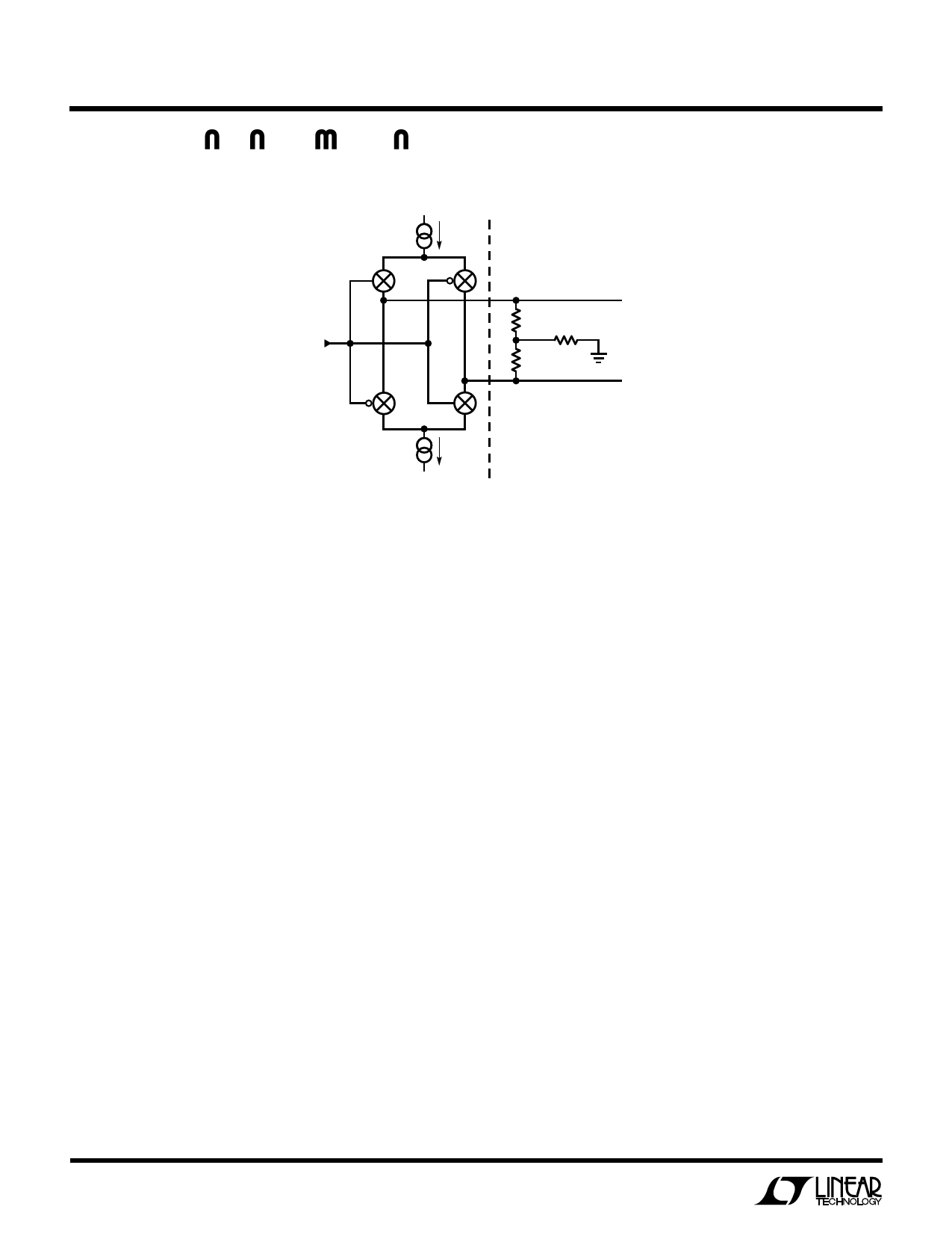
Figure 7. Simplified Transmitter Schematic
Theory of Operation
The transmitter outputs consist of complementary
switched-current sources as shown in Figure 7.
With a logic zero at the transmitter input, the inverting
output Z sources 11mA and the noninverting output Y
sinks 11mA. The differential transmitter output voltage is
then set by the termination resistors. With two differential
50Ω resistors at each end of the cable, the voltage is set to
(50Ω)(11mA) = 0.55V. With a logic 1 at the transmitter
input, output Z sinks 11mA and Y sources 11mA. The
common mode voltage of Y and Z is 0V when both current
sources are matched and there is no ground potential
difference between the cable terminations. The transmitter
current sources have a common mode range of±2V, which
allows for a ground difference between cable terminations
of ±4V.
Each receiver input has a 30k resistance to ground and
requires external termination to meet the V.35 input imped-
ance specification. The receivers have an input hysteresis
of 50mV to improve noise immunity.
Three Select pins, S0, S1 and S2, configure the chip as
described in Function Tables. When the transmitters and
receivers are OFF, all outputs are forced into high imped-
ance. The S0 pin can be used as receiver output enable.
In shutdown mode, ICC drops to 1µA with all transmitters
and receivers OFF. When the LTC1346A is enabled from
shutdown the transmitters and receivers require 2µs to
stabilize.
Complete V.35 Port
Figure 8 shows the schematic of a complete surface
mounted, ±5V DTE and DCE V.35 port using only three ICs
and six capacitors per port. The LTC1346A is used to
transmit the clock and data signals and the LT1134A to
transmit the control signals. If test signals 140, 141 and
142 are not used, the transmitter inputs should be tied
to VCC.
RS422/RS485 Applications
The receivers on the LTC1346A can be used for RS422
and RS485 applications. Using the test circuit in Figure 9,
the LTC1346A receivers are able to successfully extract
the data stream from the common mode voltage, meeting
RS422 and RS485 requirements as shown in Figures 10
and 11.
8
Share Link: 