LTC1543(RevA) View Datasheet(PDF) - Linear Technology
Part Name
Description
Manufacturer
LTC1543 Datasheet PDF : 20 Pages
| |||
LTC1543
PI FU CTIO S
C1–␣ (Pin 1): Capacitor C1 Negative Terminal. Connect a
1µF capacitor between C1+ and C1–.
C1+ (Pin 2): Capacitor C1 Positive Terminal. Connect a
1µF capacitor between C1+ and C1 –.
VDD (Pin 3): Generated Positive Supply Voltage for
V.28. Connect a 1µF capacitor to ground.
VCC (Pin 4): Positive Supply Voltage Input. 4.75V ≤ VCC
≤ 5.25V. Bypass with a 1µF capacitor to ground.
D1 (Pin 5): TTL Level Driver 1 Input.
D2 (Pin 6): TTL Level Driver 2 Input.
D3 (Pin 7): TTL Level Driver 3 Input.
R1 (Pin 8): CMOS Level Receiver 1 Output.
R2 (Pin 9): CMOS Level Receiver 2 Output.
R3 (Pin 10): CMOS Level Receiver 3 Output.
M0 (Pin 11): TTL Level Mode Select Input 0 with Pull-Up
to VCC.
M1 (Pin 12): TTL Level Mode Select Input 1 with Pull-Up
to VCC.
M2 (Pin 13): TTL Level Mode Select Input 2 with Pull-Up
to VCC.
DCE/DTE (Pin 14): TTL Level Mode Select Input with Pull-
Up to VCC.
R3 B (Pin 15): Receiver 3 Noninverting Input with Pull-Up
to VCC.
R3 A (Pin 16): Receiver 3 Inverting Input.
R2 B (Pin 17): Receiver 2 Noninverting Input.
R2 A (Pin 18): Receiver 2 Inverting Input.
D3/R1 B (Pin 19): Receiver 1 Noninverting Input and
Driver 3 Noninverting Output.
D3/R1 A (Pin 20): Receiver 1 Inverting Input and Driver 3
Inverting Output.
D2 B (Pin 21): Driver 2 Noninverting Output.
D2 A (Pin 22): Driver 2 Inverting Output.
D1 B (Pin 23): Driver 1 Noninverting Output.
D1 A (Pin 24): Driver 1 Inverting Output.
GND (Pin 25): Ground.
VEE (Pin 26): Negative Supply Voltage. Connect a 3.3µF
capacitor to GND.
C2 – (Pin 27): Capacitor C2 Negative Terminal. Connect a
1µF capacitor between C2 + and C2 –.
C2 + (Pin 28): Capacitor C2 Positive Terminal. Connect a
1µF capacitor between C2+ and C2 –.
TEST CIRCUITS
A
VOD
B
RL
50Ω
RL VOC
50Ω
1543 F01
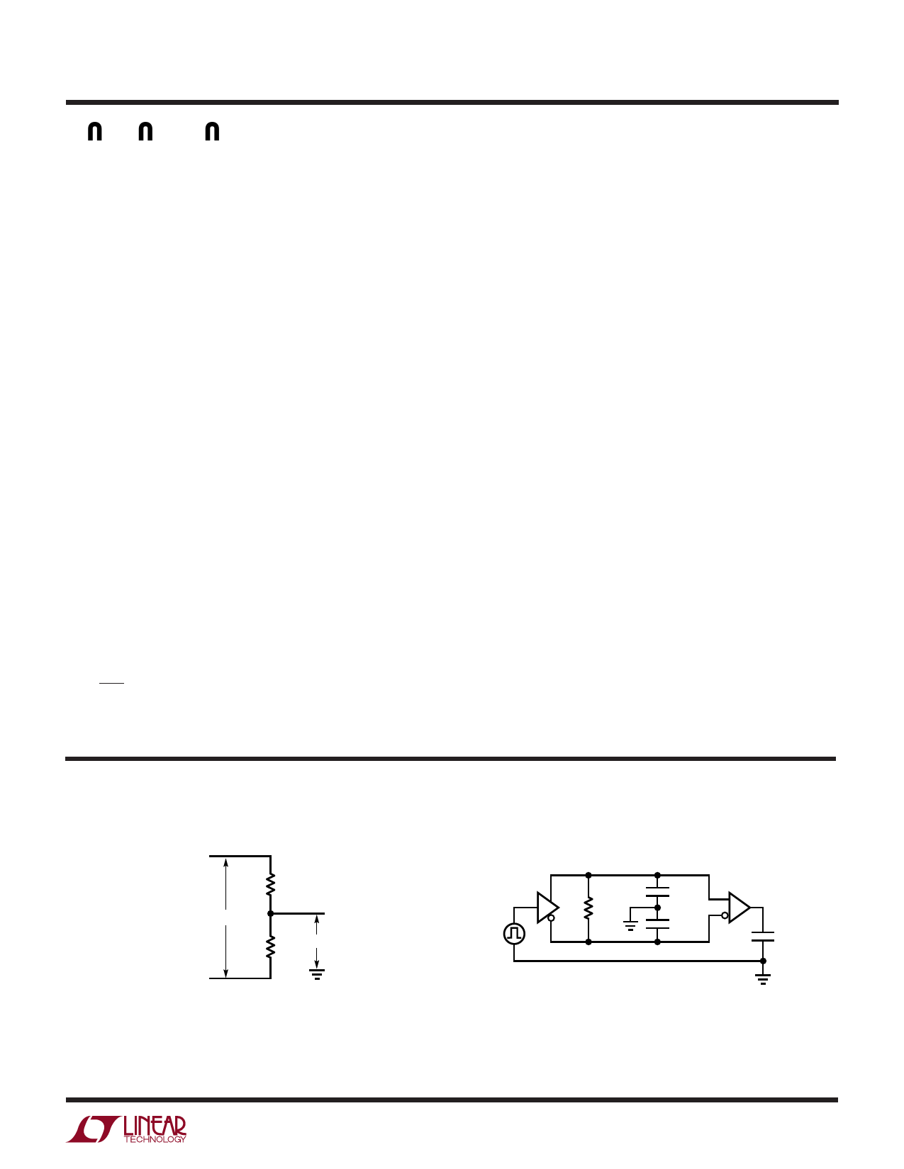
Figure 1. V.11 Driver Test Circuit
B
RL
A
100Ω
CL
100pF
B
CL
100pF
A
R
15pF
1543 F02
Figure 2. V.11 Driver/Receiver AC Test Circuit
sn1534 1543fas
5
Share Link: 