LTC2226HLX-PBF View Datasheet(PDF) - Linear Technology
Part Name
Description
Manufacturer
LTC2226HLX-PBF Datasheet PDF : 16 Pages
| |||
LTC2226H
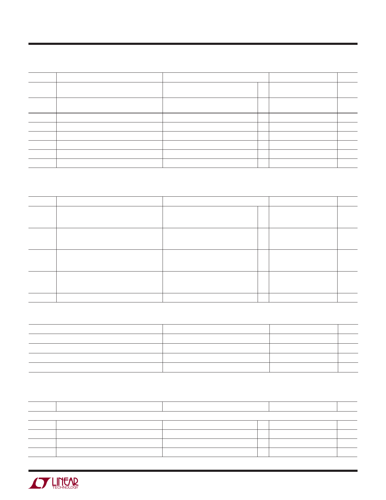
ANALOG INPUT The l denotes the speciп¬Ғcations which apply over the full operating temperature range, otherwise
speciп¬Ғcations are at TA = 25В°C. (Note 4)
SYMBOL
VIN
VIN, CM
IIN
ISENSE
IMODE
tAP
tJITTER
CMRR
PARAMETER
Analog Input Range (AIN+ вҖ“ AINвҖ“)
CONDITIONS
2.8V < VDD < 3.5V (Note 7)
Analog Input Common Mode (AIN+ + AINвҖ“)/2
Analog Input Leakage Current
SENSE Input Leakage
MODE Pin Leakage
Sample-and-Hold Acquisition Delay Time
Sample-and-Hold Acquisition Delay Time Jitter
Analog Input Common Mode Rejection Ratio
Differential Input (Note 7)
Single Ended Input (Note 7)
0V < AIN+, AINвҖ“ < VDD
0V < SENSE < 1V
MIN TYP MAX
l
Вұ0.5V to
Вұ1V
l
1
1.5
1.9
l 0.5
1.5
2
l вҖ“10
10
l вҖ“10
10
l вҖ“10
10
0
0.2
80
UNITS
V
V
V
ОјA
ОјA
ОјA
ns
psRMS
dB
DYNAMIC ACCURACY The l denotes the speciп¬Ғcations which apply over the full operating temperature range,
otherwise speciп¬Ғcations are at TA = 25В°C. AIN = вҖ“1dBFS. (Note 4)
SYMBOL PARAMETER
CONDITIONS
MIN TYP MAX UNITS
SNR
Signal-to-Noise Ratio
5MHz Input
12.5MHz Input
70MHz Input
71.4
dB
l 69.6 71.2
dB
70.9
dB
SFDR
Spurious Free Dynamic Range
2nd or 3rd Harmonic
5MHz Input
12.5MHz Input
70MHz Input
90
dB
l 74
90
dB
85
dB
SFDR
Spurious Free Dynamic Range
4th Harmonic or Higher
5MHz Input
12.5MHz Input
70MHz Input
90
dB
l 78
90
dB
90
dB
S/(N+D) Signal-to-Noise Plus Distortion Ratio
5MHz Input
12.5MHz Input
70MHz Input
71.4
dB
l 69.1 71.2
dB
70.8
dB
IMD
Intermodulation Distortion
fIN1 = 4.3MHz, fIN2 = 4.6MHz
90
dB
INTERNAL REFERENCE CHARACTERISTICS TA = 25В°C. (Note 4)
PARAMETER
CONDITIONS
VCM Output Voltage
IOUT = 0
VCM Output Tempco
VCM Line Regulation
2.8V < VDD < 3.5V
VCM Output Regulation
вҖ“1mA < IOUT < 1mA
MIN
1.475
TYP
1.500
Вұ25
3
4
MAX
1.525
UNITS
V
ppm/В°C
mV/V
О©
DIGITAL INPUTS AND DIGITAL OUTPUTS The l denotes the speciп¬Ғcations which apply over the full
operating temperature range, otherwise speciп¬Ғcations are at TA = 25В°C. (Note 4)
SYMBOL PARAMETER
LOGIC INPUTS (CLK, OE, SHDN)
CONDITIONS
MIN TYP MAX UNITS
VIH
High Level Input Voltage
VIL
Low Level Input Voltage
IIN
Input Current
CIN
Input Capacitance
VDD = 3V
VDD = 3V
VIN = 0V to VDD
(Note 7)
l
2
V
l
0.8
V
l вҖ“10
10
ОјA
3
pF
2226hfb
3
Share Link: 