LX8580A View Datasheet(PDF) - Microsemi Corporation
Part Name
Description
Manufacturer
LX8580A Datasheet PDF : 8 Pages
| |||
INTEGRATED PRODUCTS
LX8580A
7.5A Very Low Dropout Positive Regulator
PRODUCTION DATA SHEET
ABSOLUTE MAXIMUM RATINGS
VCTRL Input Voltage .........................................................................................13V
VPWR Input Voltage ............................................................................................7V
Power Dissipation ..................................................................... Internally Limited
Operating Junction Temperature.................................................................. 150°C
Storage Temperature Range...........................................................-65°C to 150°C
Lead Temperature (Soldering 180 seconds)................................................. 300°C
Note: Exceeding these ratings could cause damage to the device. All voltages are with respect to
Ground. Currents are positive into, negative out of specified terminal.
THERMAL DATA
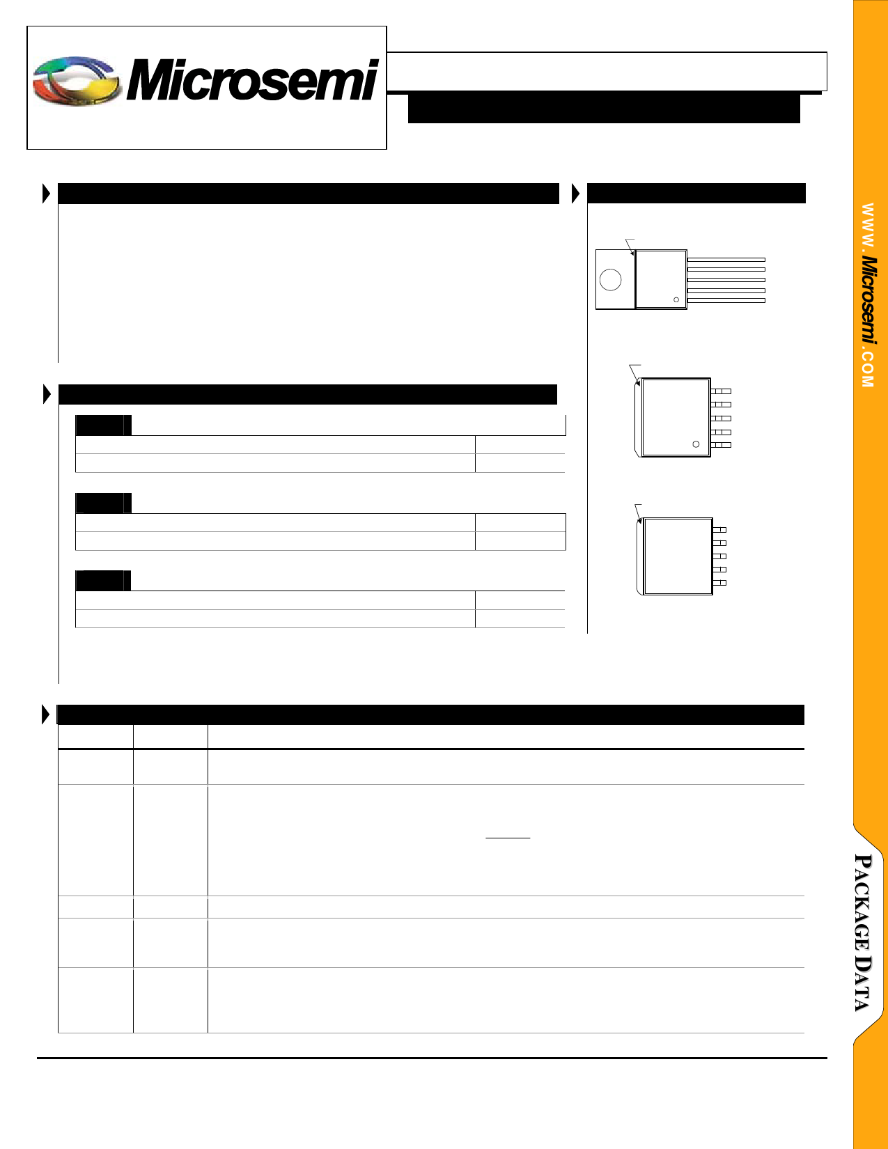
P Plastic TO-220 5-Pin
THERMAL RESISTANCE-JUNCTION TO TAB, θJT
THERMAL RESISTANCE-JUNCTION TO AMBIENT, θJA
3.0°C/W
65°C/W
DD Plastic TO-263 5-Pin
THERMAL RESISTANCE-JUNCTION TO TAB, θJT
THERMAL RESISTANCE-JUNCTION TO AMBIENT, θJA
3.0°C/W
35°C/W
DF Plastic S-Pack 5-Pin
THERMAL RESISTANCE-JUNCTION TO TAB, θJT
THERMAL RESISTANCE-JUNCTION TO AMBIENT, θJA
3.0°C/W
35°C/W
Junction Temperature Calculation: TJ = TA + (PD x θJA). θJA assume device is mounted
on a 0.5 inch2 copper pad. The θJA numbers are guidelines for the thermal performance of
the device/pc-board system. All of the above assume no ambient airflow.
PACKAGE PIN OUT
TAB is OUTPUT
5
4
3
2
1
P PACKAGE (5-PIN)
(Top View)
VPWR
VCTRL
OUTPUT
ADJUST
SENSE
TAB is OUTPUT
5
VPWR
4
VCTRL
3
OUTPUT
2
ADJUST
1
SENSE
DD PACKAGE (5-PIN)
(Top View)
TAB is OUTPUT
5
VPWR
4
VCTRL
3
OUTPUT
2
ADJUST
1
SENSE
DF PACKAGE
(Top View)
FUNCTIONAL PIN DESCRIPTION
PIN
NAME
DESCRIPTION
1
SENSE
This pin is the positive side of the reference voltage for the device. With this pin it is possible to
Kelvin-sense the output voltage at the load.
This pin is the negative side of the reference voltage for the device. Ripple rejection can be
improved by adding a small bypass capacitor from the ADJUST pin to ground. The capacitor value
should be selected so that:
2
ADJUST
1
CR ≤ 2πFRR1
where FR is the ripple frequency and R1 is the value of the resistor between the ADJUST and
SENSE leads of the LX8580A
3
OUTPUT This is the regulated power output of the device
This pin is the voltage supply pin for the control circuitry of the device. The current flow into this pin
4
VCTRL
will be about 1% of the output current. Please refer to the electrical characteristics section of
the data sheet for dropout voltage for load conditions.
This is the collector of the power section of the LX8580A. The output load current is supplied
5
VPWR
through this pin. For the device to regulate, the voltage at this pin must be between 0.1V and 0.8V
greater than the output voltage (Higher output current require higher voltages differences between
VPWR and OUTPUT).
Copyright 2001
Rev. 1.4, 2003-01-06
Microsemi
Linfinity Microelectronics Division
11861 Western Avenue, Garden Grove, CA. 92841, 714-898-8121, Fax: 714-893-2570
Page 2
Share Link: 