M27C800 View Datasheet(PDF) - STMicroelectronics
Part Name
Description
Manufacturer
M27C800 Datasheet PDF : 17 Pages
| |||
M27C800
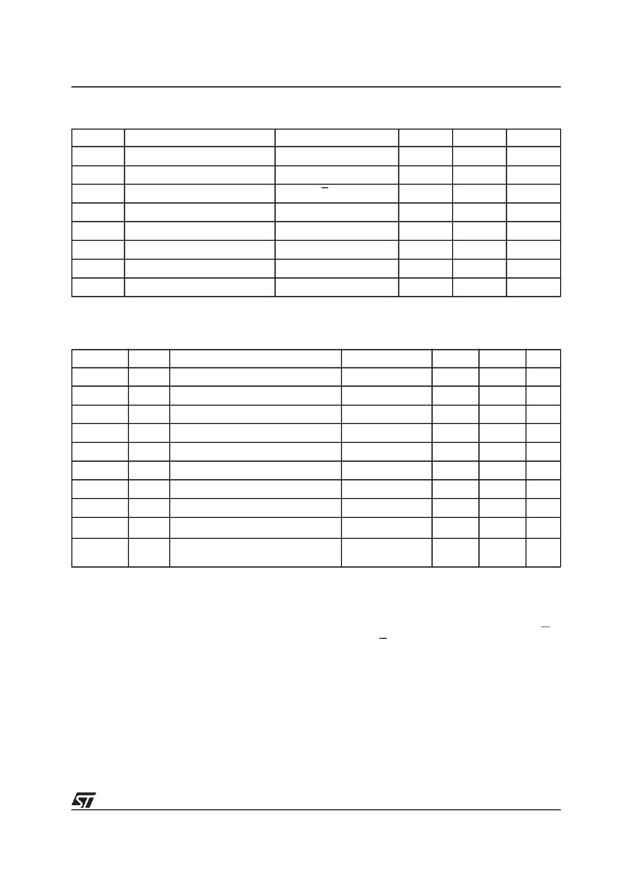
Table 9. Programming Mode DC Characteristics (1)
(TA = 25 °C; VCC = 6.25V ± 0.25V; VPP = 12.5V ± 0.25V)
Symbol
Parameter
Test Conditio n
Min
Max
Unit
ILI
Input Leakage Current
0 ≤ VIN ≤ VCC
±1
µA
ICC
Supply Current
50
mA
IPP
Program Current
E = VIL
50
mA
VIL
Input Low Voltage
–0.3
0.8
V
VIH
Input High Voltage
2.4
VCC + 0.5
V
VOL
Output Low Voltage
IOL = 2.1mA
0.4
V
VOH Output High Voltage TTL
IOH = –2.5mA
3.5
V
VID
A9 Voltage
11.5
12.5
V
Note: 1. VCC must be applied simultaneously with or before VPP and removed simultaneously or after VPP.
Table 10. Programming Mode AC Characteristics (1)
(TA = 25 °C; VCC = 6.25V ± 0.25V; VPP = 12.5V ± 0.25V)
Symbol
Alt
Parameter
Test Condition
Min
tAVEL
tAS Address Valid to Chip Enable Low
2
tQVEL
tDS Input Valid to Chip Enable Low
2
tVPHAV
tVPS VPP High to Address Valid
2
tVCHAV
tVCS VCC High to Address Valid
2
tELEH
tPW Chip Enable Program Pulse Width
45
tEHQX
tDH Chip Enable High to Input Transition
2
tQXGL
tOES Input Transition to Output Enable Low
2
tGLQV
tOE Output Enable Low to Output Valid
tGHQZ (2)
tDFP Output Enable High to Output Hi-Z
0
tGHAX
tAH
Output Enable High to Address
Transition
0
Note: 1. VCC must be applied simultaneously with or before VPP and removed simultaneously or after VPP.
2. Sampled only, not 100% tested.
Max Unit
µs
µs
µs
µs
55
µs
µs
µs
120
ns
130
ns
ns
Programming
When delivered (and after each erasure for UV
EPROM), all bits of the M27C800 are in the ’1’
state. Data is introduced by selectively program-
ming ’0’s into the desired bit locations. Although
only ’0’s will be programmed, both ’1’s and ’0’s can
be present in the data word. The only way to
change a ’0’ to a ’1’ is by die exposition to ultravio-
let light (UVEPROM). The M27C800 is in the pro-
gramming mode when VPP input is at 12.5V, G is
at VIH and E is pulsed to VIL. The data to be pro-
grammed is applied to 16 bits in parallel to the data
output pins. The levels required for the address
and data inputs are TTL. VCC is specified to be
6.25V ± 0.25V.
9/17
Share Link: 