M29F200 View Datasheet(PDF) - STMicroelectronics
Part Name
Description
Manufacturer
M29F200 Datasheet PDF : 33 Pages
| |||
M29F200T, M29F200B
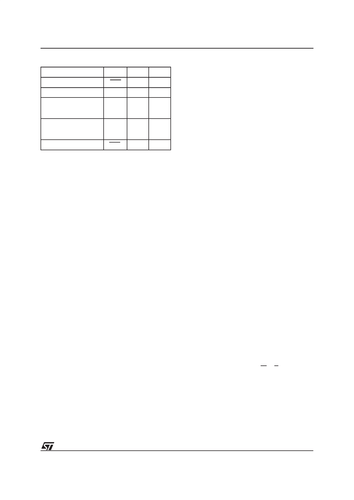
Table 10. Polling and Toggle Bits
Mode
DQ7 DQ6 DQ2
Program
DQ7 Toggle 1
Erase
Erase Suspend Read
(in Erase Suspend
block)
0
Toggle Note 1
1
1 Toggle
Erase Suspend Read
(outside Erase Suspend
block)
DQ7
DQ6
DQ2
Erase Suspend Program DQ7 Toggle N/A
Note: 1. Toggle if the address is within a block being erased.
’1’ if the address is within a block not being erased.
Toggle Bit (DQ2). This toggle bit, together with
DQ6, can be used to determine the device status
during the Erase operations. It can also be used to
identify the block being erased. During Erase or
Erase Suspend a read from a block being erased
will cause DQ2 to toggle. A read from a block not
being erased will set DQ2 to ’1’ during erase and
to DQ2 during Erase Suspend. During Chip Erase
a read operation will cause DQ2 to toggle as all
blocks are being erased. DQ2 will be set to ’1’
during program operation and when erase is com-
plete. After erase completion and if the error bit
DQ5 is set to ’1’, DQ2 will toggle if the faulty block
is addressed.
Error Bit (DQ5). This bit is set to ’1’ by the P/E.C.
when there is a failure of programming, block
erase, or chip erase that results in invalid data in
the memory block. In caseof an error in block erase
or program, the block in which the error occured or
to which the programmed data belongs, must be
discarded. The DQ5 failure condition will also ap-
pear if a user tries to program a ’1’ to a locationthat
is previously programmed to ’0’. Other Blocks may
stillbe used.The error bit resets after a Read/Reset
(RD) instruction. In case of success of Program or
Erase, the error bit will be set to ’0’ .
Erase Timer Bit (DQ3). This bit is set to ’0’ by the
P/E.C. when the last block Erase command has
been entered to the Command Interface and it is
awaiting the Erase start. When the erase timeout
period is finished, after 80µs to 120µs, DQ3 returns
to ’1’.
Coded Cycles
The two Coded cycles unlock the Command Inter-
face. They are followed by an input command or a
confirmation command. The Coded cycles consist
of writing the data AAh at address AAAAh in the
Byte-wide configuration and at address 5555h in
the Word-wide configuration during the first cycle.
During the second cycle the Coded cycles consist
of writing the data 55h at address 5555h in the
Byte-wide configuration and at address 2AAAh in
the Word-wide configuration. In the Byte-widecon-
figuration the address lines A–1 to A14 are valid, in
Word-wide A0 to A14 are valid, other address lines
are ’don’t care’. The Coded cycles happen on first
and second cycles of the command write or on the
fourth and fifth cycles.
Instructions
See Table 8.
Read/Reset (RD) Instruction. The Read/Reset
instruction consists of one write cycle giving the
command F0h. It can be optionally preceded by the
two Coded cycles. Subsequentread operationswill
read the memory array addressed and output the
data read. A wait state of 10µs is necessary after
Read/Reset prior to any valid read if the memory
was in an Erase mode when the RD instruction is
given.
Auto Select (AS) Instruction. This instruction
uses the two Coded cycles followed by one write
cycle giving the command 90h to address AAAAh
in the Byte-wide configuration or address 5555h in
the Word-wide configuration for command set-up.
A subsequent read will output the manufacturer
code and the device code or the block protection
status depending on the levels of A0 and A1. The
manufacturer code, 20h, is output when the ad-
dresses lines A0 and A1 are Low, the device code,
D3h for Top Boot, D4h for Bottom Boot is output
when A0 is High with A1 Low.
The AS instruction also allows access to the block
protectionstatus.After givingthe AS instruction, A0
is set to VIL with A1 at VIH, while A12-A16 define
the address of the block to be verified. A read in
these conditions will output a 01h if the block is
protected and a 00h if the block is not protected.
Program (PG) Instruction. This instruction uses
four write cycles. Both for Byte-wide configuration
and for Word-wide configuration. The Program
command A0h is written to address AAAAh in the
Byte-wide configuration or to address 5555h in the
Word-wide configurationon the third cycle after two
Coded cycles. A fourth write operation latches the
Address on the falling edge of W or E and the Data
to be written on the rising edge and starts the
P/E.C. Read operations output the Status Register
bits after the programming has started. Memory
programming is made only by writing ’0’ in place of
’1’. Status bits DQ6 and DQ7 determine if program-
ming is on-goingand DQ5 allows verification of any
possible error. Programming at an address not in
blocks being erased is also possible during erase
suspend. In this case, DQ2 will toggle at the ad-
dress being programmed.
11/33
Share Link: 