M29W017D View Datasheet(PDF) - STMicroelectronics
Part Name
Description
Manufacturer
M29W017D Datasheet PDF : 36 Pages
| |||
M29W017D
Array mode, or when the device is in Autoselected
mode.
One Bus Write cycle is required to issue the Read
CFI Query Command. Once the command is is-
sued subsequent Bus Read operations read from
the Common Flash Interface Memory Area.
The Read/Reset command must be issued to re-
turn the device to the previous mode (the Read Ar-
ray mode or Autoselected mode). A second Read/
Reset command would be needed if the device is
to be put in the Read Array mode from Autoselect-
ed mode.
See Appendix B, Tables 17, 18, 19, 20, 21 and 22
for details on the information contained in the
Common Flash Interface (CFI) memory area.
Block Protect and Chip Unprotect Commands.
Each block can be separately protected against
accidental Program or Erase. The whole chip can
be unprotected to allow the data inside the blocks
to be changed.
Block Protect and Chip Unprotect operations are
described in Appendix C.
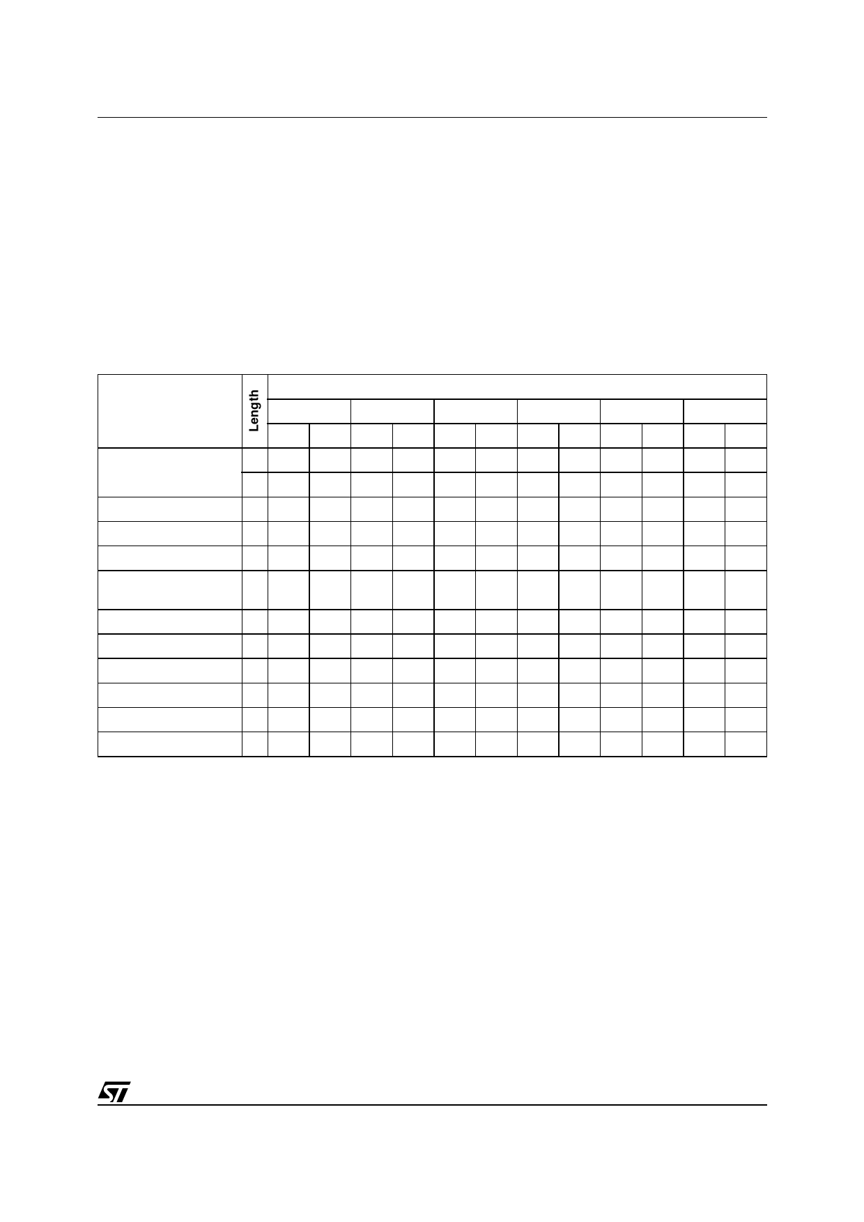
Table 3. Commands
Bus Write Operations
Command
1st
2nd
3rd
4th
5th
6th
Addr Data Addr Data Addr Data Addr Data Addr Data Addr Data
Read/Reset
1 x F0
3 x AA x 55 x F0
Auto Select
3 x AA x 55 x 90
Program
4 x AA x 55 x A0 PA PD
Unlock Bypass
3 x AA x 55 x 20
Unlock Bypass
Program
2 x A0 PA PD
Unlock Bypass Reset 2 x 90 x 00
Chip Erase
6 x AA x 55 x 80 x AA x 55 x 10
Block Erase
6+ x AA x 55 x 80 x AA x 55 BA 30
Erase Suspend
1 x B0
Erase Resume
1 x 30
Read CFI Query
1 55 98
Note: x Don’t Care, PA Program Address, PD Program Data, BA Any address in the Block. All values in the table are in hexadecimal.
13/36
Share Link: 