M2V28S20TP View Datasheet(PDF) - Mitsumi
Part Name
Description
Manufacturer
M2V28S20TP Datasheet PDF : 52 Pages
| |||
SDRAM (Rev. 1.0E)
Jun. '99
MITSUBISHI LSIs
M2V28S20TP-6,-7,-8
M2V28S30TP-6,-7,-7L,-8,-8L
M2V28S40TP-7,-7L,-8,-8L
128M Synchronous DRAM
(4-BANK x 8,388,608-WORD x 4-BIT)
(4-BANK x 4,194,304-WORD x 8-BIT)
(4-BANK x 2,097,152-WORD x 16-BIT)
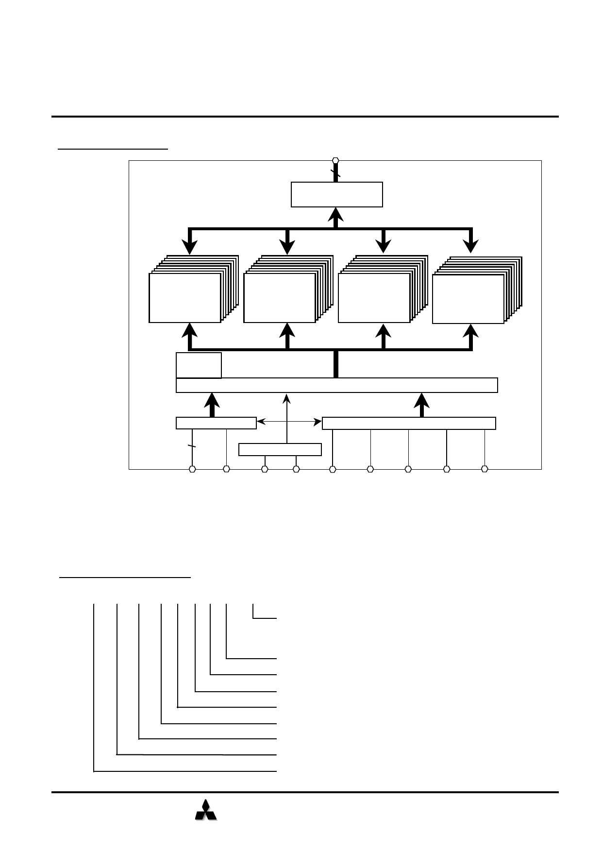
BLOCK DIAGRAM
DQ0-7
I/O Buffer
Memory Array
4096 x1024 x8
Cell Array
Bank #0
Memory Array
4096 x1024 x8
Cell Array
Bank #1
Memory Array
4096 x1024 x8
Cell Array
Bank #2
Memory Array
4096 x1024 x8
Cell Array
Bank #3
Mode
Register
Control Circuitry
Address Buffer
Clock Buffer
Control Signal Buffer
A0-11 BA0,1
CLK CKE
/CS /RAS
/CAS
/WE DQM
Note : This figure shows the M2V28S30TP.
The M2V28S20TP configration is 4096x2048x4 of cell array and DQ 0-3.
The M2V28S40TP configration is 4096x512x16 of cell array and DQ 0-15.
Type Designation Code
M2 V 28 S 3 0
TP -8
These rules are only applied to the Synchronous DRAM family.
Access Item
Package Type
Process Generation
Function
Organization
Synchronous DRAM
Density
Interface
Mitsubishi DRAM
-6 : 7.5ns (PC133/3-3-3),
-7 : 10ns(PC100/2-2-2),
-8 : 10ns(PC100/3-2-2)
TP : TSOP(II)
Blank : 1st gen.
0 : Random Column
2: x4, 3: x8, 4: x16
28 : 128Mbit
V : LVTTL
MITSUBISHI ELECTRIC
4
Share Link: 