M34551 View Datasheet(PDF) - MITSUBISHI ELECTRIC
Part Name
Description
Manufacturer
M34551
MITSUBISHI ELECTRIC

M34551 Datasheet PDF : 68 Pages
| |||
MITSUBISHI MICROCOMPUTERS
4551 Group
SINGLE-CHIP 4-BIT CMOS MICROCOMPUTER for
INFRARED REMOTE CONTROL TRANSMITTER
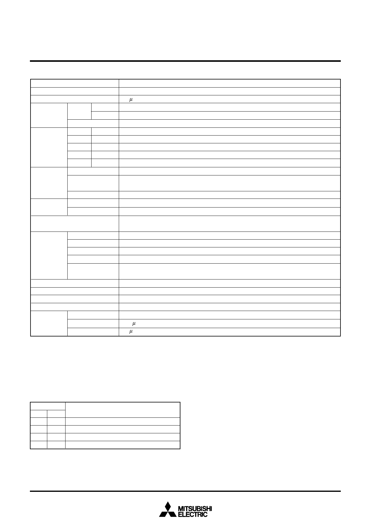
PERFORMANCE OVERVIEW
Parameter
Function
Number of basic instructions
92
Minimum instruction execution time 1.5 µs (f(XIN) = 8.0 MHz:system clock = f(XIN)/4: VDD = 5.0 V)
Memory sizes ROM M34551M4 4096 words ! 10 bits
M34551E8 8192 words ! 10 bits
RAM
280 words ! 4 bits (LCD RAM 20 words ! 4 bits included)
Input/Output D0–D7 Output Eight independent output ports
ports
P00–P03 I/O
4-bit I/O port; each pin is equipped with a pull-up function.
P10–P13 I/O
4-bit I/O port; each pin is equipped with a pull-up function.
P20–P23 Input
4-bit input port
CARR Output 1-bit output port (CMOS output)
Timers
Timer 1
8-bit timer with a reload register
Timer 2/
14-bit timer/
Watchdog timer Fixed dividing frequency timer
Timer LC
4-bit timer with a reload register
Interrupt
Sources
3 (one for external and two for timer)
Nesting
1 level
Subroutine nesting
8 levels (however, only 7 levels can be used when an interrupt is used or the TABP p instruction
is executed)
LCD
Selective bias value 1/2, 1/3 bias
Selective duty value 2, 3, 4 duty
Common output 4
Segment output 20
Internal resistor for 200 kΩ ! 3
power supply
Device structure
CMOS silicon gate
Package
48-pin plastic molded QFP
Operating temperature range
–20 °C to 70 °C
Supply voltage
2.2 V to 5.5 V (One Time PROM version: 2.5 V to 5.5 V)
Power
at active
2.5 mA (f(XIN) = 8.0 MHz system clock = f(XIN)/4, VDD=5 V)
dissipation at clock operating 27.5 µA (at main clock oscillation stop, sub-clock oscillation frequency: 32.0 kHz, VDD=5 V)
(typical value) at RAM back-up 0.1 µA (at main clock oscillation stop, sub-clock oscillation stop, Ta=25 °C, VDD=5V)
DEFINITION OF CLOCK AND CYCLE
q System clock (STCK)
The system clock is the basic clock for controlling this product.
The system clock can be selected by bits 0 and 3 of the clock
control register MR as shown in the table below.
Table Selection of system clock
Register MR
MR3 MR0
System clock (STCK)
0
0 f(XIN)
0
1 f(XCIN)
1
0 f(XIN)/4
1
1 f(XCIN)/4
Note: f(XIN)/4 is selected immediately after system is released
from reset.
q Instruction clock (INSTK)
The instruction clock is the standard clock for controlling CPU.
The instruction clock is a signal derived from dividing the
system clock by 3. The one cycle of the instruction clock is
equivalent to the one machine cycle.
q Machine cycle
The machine cycle is the standard cycle required to execute
the instruction.
3
Share Link: