ICPL2601 View Datasheet(PDF) - Isocom
Part Name
Description
Manufacturer
ICPL2601 Datasheet PDF : 4 Pages
| |||
SWITCHING SPECIFICATIONS AT TA = 25°C ( VCC = 5V, IF = 7.5mA Unless otherwise noted )
PARAMETER
Propagation Delay Time
to Logic Low at Output
( fig 1 )( note4 )
SYM DEVICE MIN TYP MAX UNITS TEST CONDITION
t
PHL
55 75 ns
R
L
=
350Ω,
C
L
=
15pF
Propagation Delay Time
to Logic High at Output
tPLH
( fig 1 )( note5 )
45 75 ns
RL = 350Ω, CL = 15pF
Propagation Delay Time
of Enable from VEH to VEL
tEHL
( note6 )
14
ns
RL = 350Ω, CL = 15pF
VEL = 0V, VEH = 3V
Propagation Delay Time
of Enable from V to V
t
EL
EH
ELH
( note7 )
25
ns
R
L
=
350Ω,
C
L
=
15pF
VEL = 0V, VEH = 3V
Common Mode Transient
Immunity at Logic High
CM 6N137
10000
H
Level Output ( fig 2 )( note8 )
ICPL2601 1000 10000
V/µs
V/µs
I = 0mA, V = 50V
F
CM
PP
RL= 350Ω,VOH= 2Vmin.
Common Mode Transient
Immunity at Logic Low
Level Output ( fig 2 )( note9 )
CM 6N137
-10000
L
ICPL2601 -1000 -10000
V/µs
V/µs
V = 50V
CM
PP
RL=350Ω,VOL=0.8Vmax.
NOTES:-
1 Bypassing of the power supply line is required, with a 0.01µF ceramic disc capacitor adjacent to
each isolator. The power supply bus for the isolator(s) should be seperate from the bus for any
active loads. Otherwise a larger value of bypass capacitor (up to 0.1µF) may be needed to supress
regenerative feedback via the power supply.
2 Peaking circuits may produce transient input currents up to 50mA, 50ns maximum pulse width,
provided average current does not exceed 20mA.
3 Device considered a two terminal device; pins 1, 2, 3, and 4 shorted together, and pins 5, 6, 7
and 8 shorted together.
4 The tPHL propagation delay is measured from the 3.75 mA level Low to High transition of the input
current pulse to the 1.5V level on the High to Low transition of the output voltage pulse.
5 The tPLH propagation delay is measured from the 3.75mA level High to Low transition of the input
current pulse to the 1.5V level on the Low to High transition of the output voltage pulse.
6 The tEHL enable input propagation delay is measured from the 1.5V level on the Low to High transition of
the enable input voltage pulse to the 1.5V level on the High to Low of the output voltage pulse.
7 The tELH enable input propagation delay is measured from the 1.5V level on the High to Low transition of
the enable input voltage pulse to the 1.5V level on the Low to High of the output voltage pulse.
8 CMH is the maximum tolerable rate of rise of the common mode voltage to assure that the output
will remain in a high logic state (ie Vout > 2.0V).
9 CML is the maximum tolerable rate of fall of the common mode voltage to assure that the output
will remain in a low logic state (ie Vout < 0.8V)
10 No external pull up is required for a high logic state on the enable input.
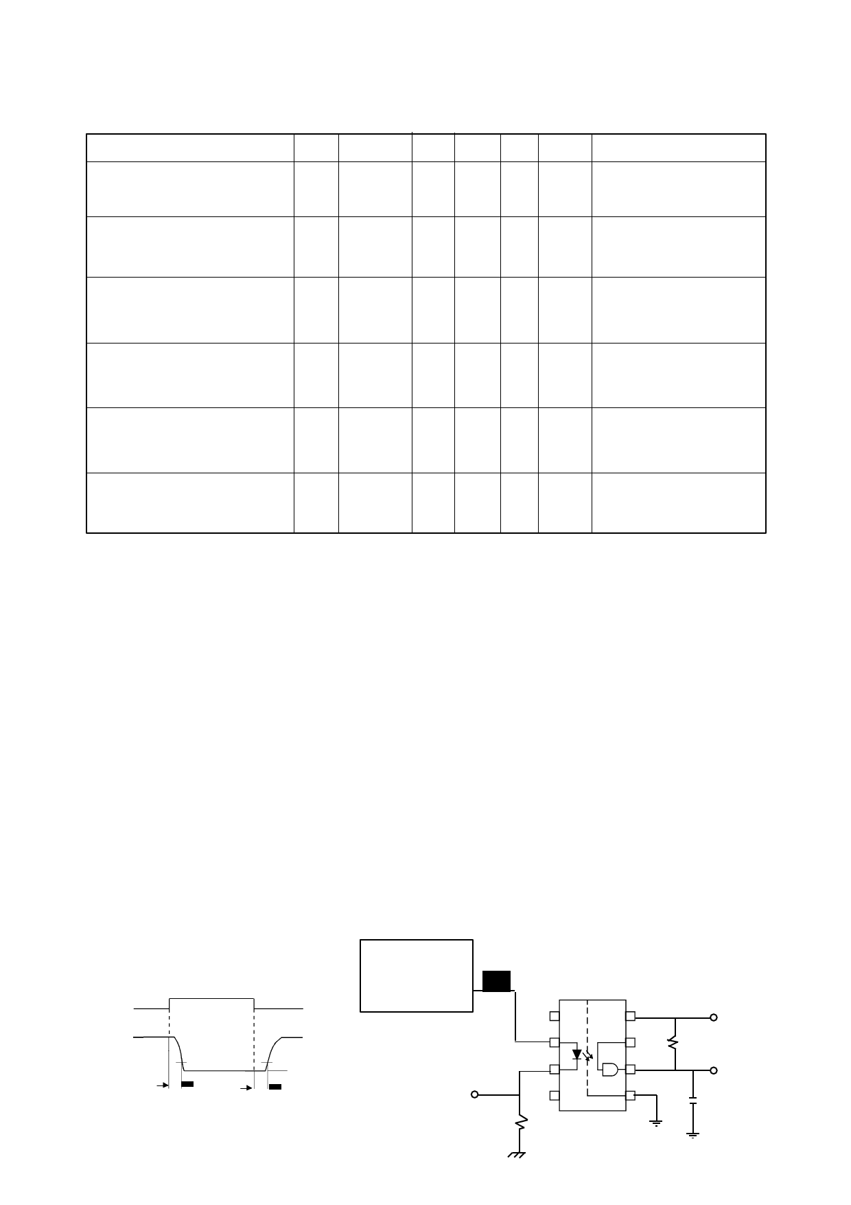
IF
0
V
O
t
PHL
FIG.1 SWITCHING TEST CIRCUIT
1.5V
t
PLH
5V
1.5V
VOL
PULSE
GENERATOR I
Z
O
=
50Ω
F
tr = 5ns
1
10% Duty Cycle
1/f < 100µs
2
3
I Monitor
4
F
100Ω
8
5V
7
RL
6
VO
5
CL = 15pF
19/4/99
DB91063-AAS/A1
Share Link: 