MASW-000834-000SMB View Datasheet(PDF) - M/A-COM Technology Solutions, Inc.
Part Name
Description
Manufacturer
MASW-000834-000SMB
M/A-COM Technology Solutions, Inc.

MASW-000834-000SMB Datasheet PDF : 4 Pages
| |||
MASW-000834-000SMB Sample Board
Application Note on Sample Board Operation of the
MASW-000834-13560T T/R Switch
M/A-COM Products
REV.3
Dual Positive and Negative Voltage
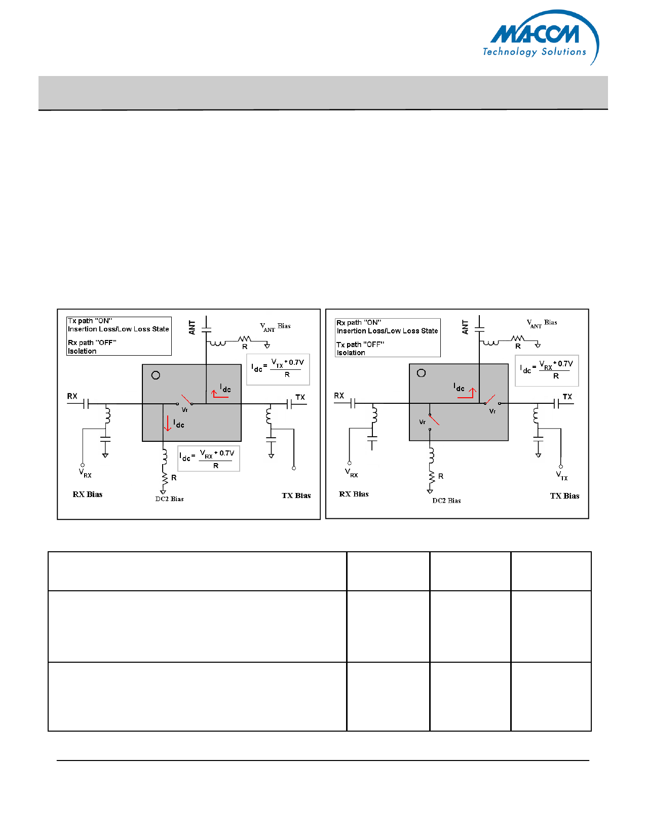
The sample board can accommodate dual polarity supplies as shown in Figures 8 through 10. In this
scheme, bias is applied to the Rx , Tx, and DC2 path. Unlike the single positive polarity bias scheme,
bias to the ANT port is not used. A series resistor on the ANT arm and second resistor on the DC2 path
will limit the current when a negative voltage is applied to the TX or RX Port. M/A-COM Tech
supplies 100 Ohm resistors on these sample boards.
In order to achieve proper isolation in the “OFF” arm, the back bias (Vr) on the diodes should be large
enough to sustain higher power levels. The voltage levels can range from +5V to +25V, as shown in
the Figure. Minimum back bias requirements will change depending on incident peak RF Voltage and
frequency of operation. Please contact M/A-COM Technology Solutions for additional guidance on
required reverse bias voltages for specific application environments.
Figure 8. Transmit On, Receive Off
Figure 9. Transmit Off, Receive On
DC BIAS
Example
Dual Bias
Scheme
Tx - Antenna Rx - Antenna
RF Condition RF Condition
VTX = Negative voltage in which ANT resistor limits current
to IDC [ANT to TX Path ON]
VRX = Positive voltage level, greater than 0V in which DC2
resistor limits current to IDC [RX Path OFF / DC2 Path On]
VANT = 0V
VTX = -5V
VRX = +25V
DC2 = 0V
IDC = +/- 50mA
Low Loss
Isolation
VRX = Negative Voltage in which ANT resistor limits current
to IDC [ANT to RX Path ON]
VTX = Positive voltage level, greater than 0V in which DC2
resistor limits current to IDC [RX Path OFF / DC2 Path On]
VANT = 0V
VRX = -5V
VTX = +25V
DC2 = 0V
IDC = +/- 50mA
Isolation
Low Loss
Figure 10. Dual Positive and Negative Voltage Source Bias Truth Table
4
M/A-COM Inc. and its affiliates reserve the right to make changes to the product(s) or information
contained herein without notice. M/A-COM makes no warranty, representation or guarantee
regarding the suitability of its products for any particular purpose, nor does M/A-COM assume any
liability whatsoever arising out of the use or application of any product(s) or information.
• North America Tel: 800.366.2266 / Fax: 978.366.2266
• Europe Tel: 44.1908.574.200 / Fax: 44.1908.574.300
• Asia/Pacific Tel: 81.44.844.8296 / Fax: 81.44.844.8298
Visit www.macom.com for additional data sheets and product information.
Share Link: