MAX1153BEUE(2010) View Datasheet(PDF) - Maxim Integrated
Part Name
Description
Manufacturer
MAX1153BEUE
(Rev.:2010)
(Rev.:2010)
Maxim Integrated

MAX1153BEUE Datasheet PDF : 30 Pages
| |||
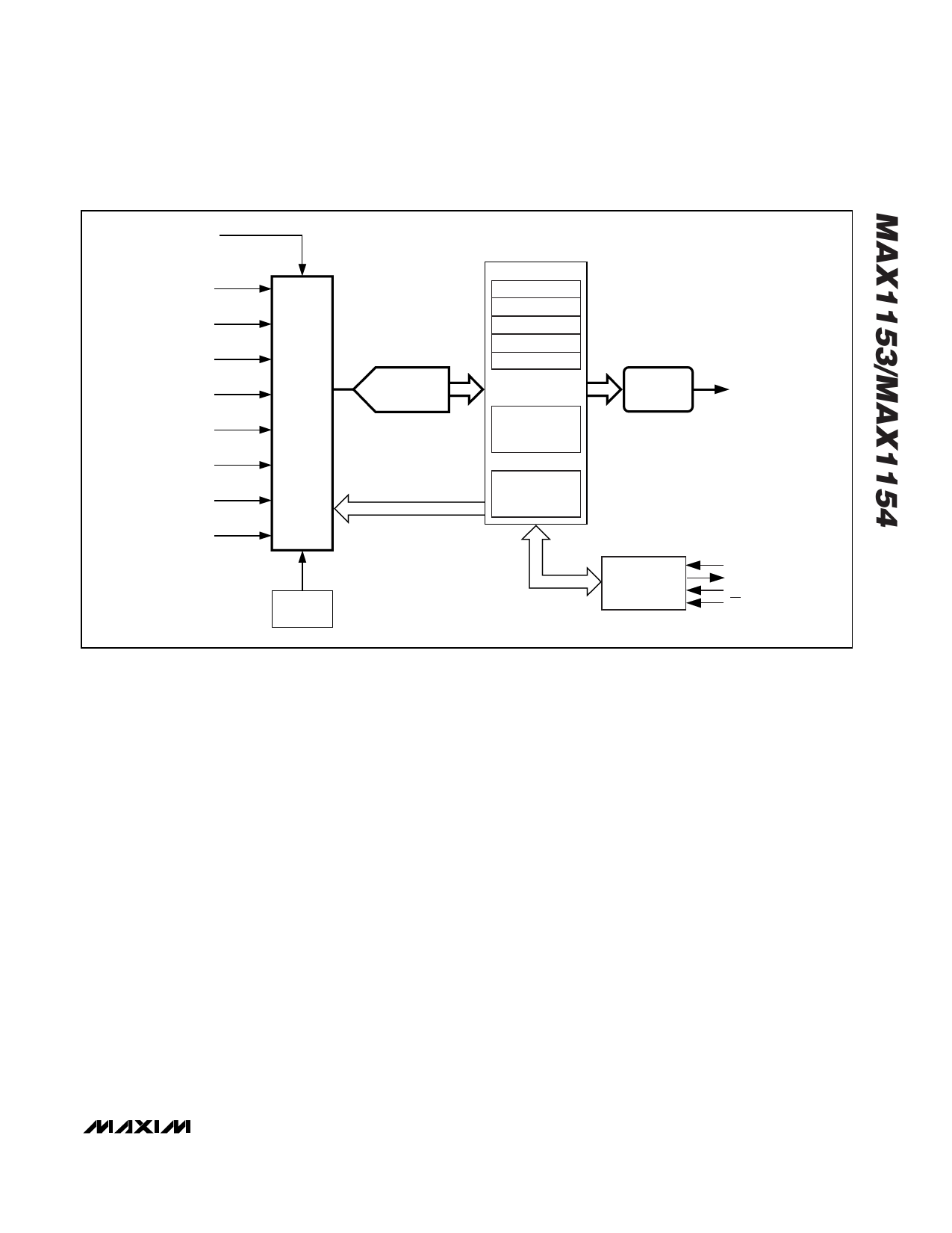
Stand-Alone, 10-Channel, 10-Bit System Monitors
with Internal Temperature Sensor and VDD Monitor
VDD
INPUT REGISTERS 0–10
AIN 0
CURRENT DATA
UPPER THRESHOLD
AIN 1
LOWER THRESHOLD
# FAULT CYCLES
AIN 2
AVERAGE
AIN 3
MUX
12-BIT
ADC WITH T/H
DIGITAL
COMPARATOR
INT
CONFIGURATION/
AIN 4
STATUS
REGISTERS
AIN 5
SCAN AND
AIN 6
CONVERSION
CONTROL
AIN 7
TEMP
SENSE
SERIAL
INTERFACE
DIN
DOUT
SCLK
CS
Figure 3. Simplified Alarm Block Diagram of the MAX1153/MAX1154
During the acquisition interval, IN+ and IN- charge both
a positive (CHOLDP) and a negative (CHOLDN) sam-
pling capacitor. After completing the acquisition inter-
val, the T/H switches open, storing an accurate sample
of the differential voltage between IN+ and IN-. This
charge is then transferred to the ADC and converted.
Finally, the conversion result is transferred to the cur-
rent data register.
Temperature conversions require 46µs (typ) and mea-
sure the difference between two sequential voltage
measurements (see the Temperature Measurement
section for a detailed description).
Fully Differential Track/Hold (T/H)
The T/H acquisition interval begins with the rising edge
of CS (for manually triggered conversions) and is inter-
nally timed to 1.5µs (typ). The accuracy of the input sig-
nal sample is a function of the input signal’s source
impedance and the T/H’s capacitance. In order to
achieve adequate settling of the T/H, limit the signal
source impedance to a maximum of 1kΩ.
Input Bandwidth
The ADC’s input tracking circuitry has a 1MHz small-
signal bandwidth. To avoid high-frequency signals
aliasing into the frequency band of interest, anti-alias
prefiltering of the input signals is recommended.
Analog Input Protection
Internal protection diodes, which clamp the analog
inputs to VDD and GND, allow the channel input pins to
swing from (VGND - 0.3V) to (VDD + 0.3V) without dam-
age. However, for accurate conversions near full scale,
the inputs must not exceed VDD by more than 50mV or
be lower than VGND by 50mV. If the analog input range
must exceed 50mV beyond the supplies, limit the input
current.
Single Ended/Differential
The MAX1153/MAX1154 use a fully differential ADC for
all conversions. Through the input configuration regis-
ter, the analog inputs can be configured for either dif-
ferential or single-ended conversions. When sampling
signal sources close to the MAX1153/MAX1154, single-
ended conversion is generally sufficient. Single-ended
conversions use only one analog input per signal
source, internally referenced to GND.
______________________________________________________________________________________ 11
Share Link: