MAX16903SAUE View Datasheet(PDF) - Maxim Integrated
Part Name
Description
Manufacturer
MAX16903SAUE Datasheet PDF : 15 Pages
| |||
MAX16903
2.1MHz, High-Voltage,
1A Mini-Buck Converter
Extended Input Voltage Range
In some cases, the MAX16903 is forced to deviate from
its operating frequency independent of the state of SYNC.
For input voltages above 18V, the required duty cycle to
regulate its output may be smaller than the minimum on-
time (80ns, typ). In this event, the MAX16903 is forced to
lower its switching frequency by skipping pulses.
If the input voltage is reduced and the MAX16903 approach-
es dropout the device tries to turn on the high-side FET
continuously. In order to maintain gate charge on the
high-side FET, the BST capacitor must be periodically
recharged. To ensure proper charge on the BST capaci-
tor when in dropout, the high-side FET is turned off every
6.5μs and the low-side FET is turned on for about 150ns.
This gives an effective duty cycle of > 97% and a switching
frequency of 150kHz when in dropout.
Spread-Spectrum Option
The MAX16903 has an optional spread-spectrum version.
If this option is selected, then the internal operating fre-
quency varies by +6% relative to the internally generated
operating frequency of 2.1MHz (typ). Spread spectrum is
offered to improve EMI performance of the MAX16903.
By varying the frequency 6% only in the positive
direction, the MAX16903 still guarantees that the 2.1MHz
frequency does not drop into the AM band limit of 1.8MHz.
Additionally, with the low minimum on-time of 80ns (typ)
no pulse skipping is observed for a 5V output with 18V
input maximum battery voltage in steady state.
The internal spread spectrum does not interfere with the
external clock applied on the SYNC pin. It is active only
when the MAX16903 is running with internally generated
switching frequency.
Power-Good (PGOOD)
The MAX16903 features an open-drain power-good out-
put. PGOOD is an active-high output that pulls low when
the output voltage is below 91% of its nominal value.
PGOOD is high impedance when the output voltage is
above 93% of its nominal value. Connect a 20kΩ (typ)
pullup resistor to an external supply or the on-chip BIAS
output.
Overcurrent Protection
The MAX16903 limits the peak output current to 1.5A
(typ). The accuracy of the current limit is ±15%, which
makes selection of external components very easy.
To protect against short-circuit events, the MAX16903
will shut off when OUTS is below 1.5V (typ) and one
overcurrent event is detected. The MAX16903 attempts
a soft-start restart every 30ms and stays off if the short
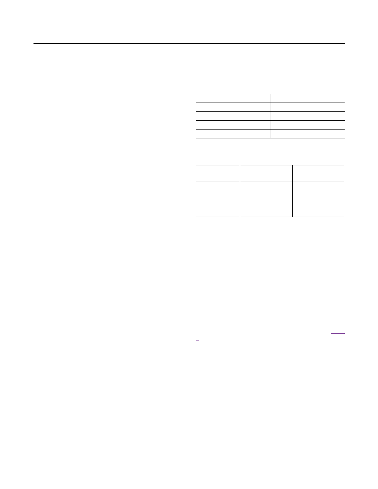
Table 1. Nominal Output Voltage Values
VOUT (V)
1.8 to 3.1
3.2 to 6.5
6.6 to 8.1
8.2 to 10
LNOM (µH)
VOUT/0.55
VOUT/0.96
VOUT/1.40
VOUT/1.75
Table 2. Examples for Standard Output
Voltages
VOUT (V)
1.8
3.3
5.0
8.0
CALCULATED
LNOM (µH)
3.3
3.4
5.2
5.7
STANDARD
VALUE (µH)
3.3
3.3
4.7
5.6
circuit has not been removed. When the current limit
is no longer present, it reaches the output voltage by
following the normal soft-start sequence. If the MAX16903
die reaches the thermal limit of 175°C (typ) during the
current-limit event, it immediately shuts off.
Thermal-Overload Protection
The MAX16903 features thermal-overload protection. The
device turns off when the junction temperature exceeds
+175°C (typ). Once the device cools by 15°C (typ), it turns
back on with a soft-start sequence.
Applications Information
Inductor Selection
The nominal inductor value can be calculated using Table
1 based on the nominal output voltage of the device.
Select the nearest standard inductance value to the calcu-
lated nominal value. The nominal standard value selected
should be within ±25% of LNOM for best performance.
Input Capacitor
A low-ESR ceramic input capacitor of 1μF or larger is
needed for proper device operation. This value may need
to be larger based on application input-voltage ripple
requirements.
The discontinuous input current of the buck converter
causes large input ripple current. The switching frequen-
cy, peak inductor current, and the allowable peak-to-peak
input-voltage ripple dictate the input capacitance require-
ment. Increasing the switching frequency or the inductor
www.maximintegrated.com
Maxim Integrated │ 10
Share Link: 