MAX832 View Datasheet(PDF) - Maxim Integrated
Part Name
Description
Manufacturer
MAX832
Maxim Integrated

MAX832 Datasheet PDF : 5 Pages
| |||
5V/3.3V/3V/Adjustable-Output, 1A,
Step-Down, PWM, Switch-Mode DC-DC Regulators
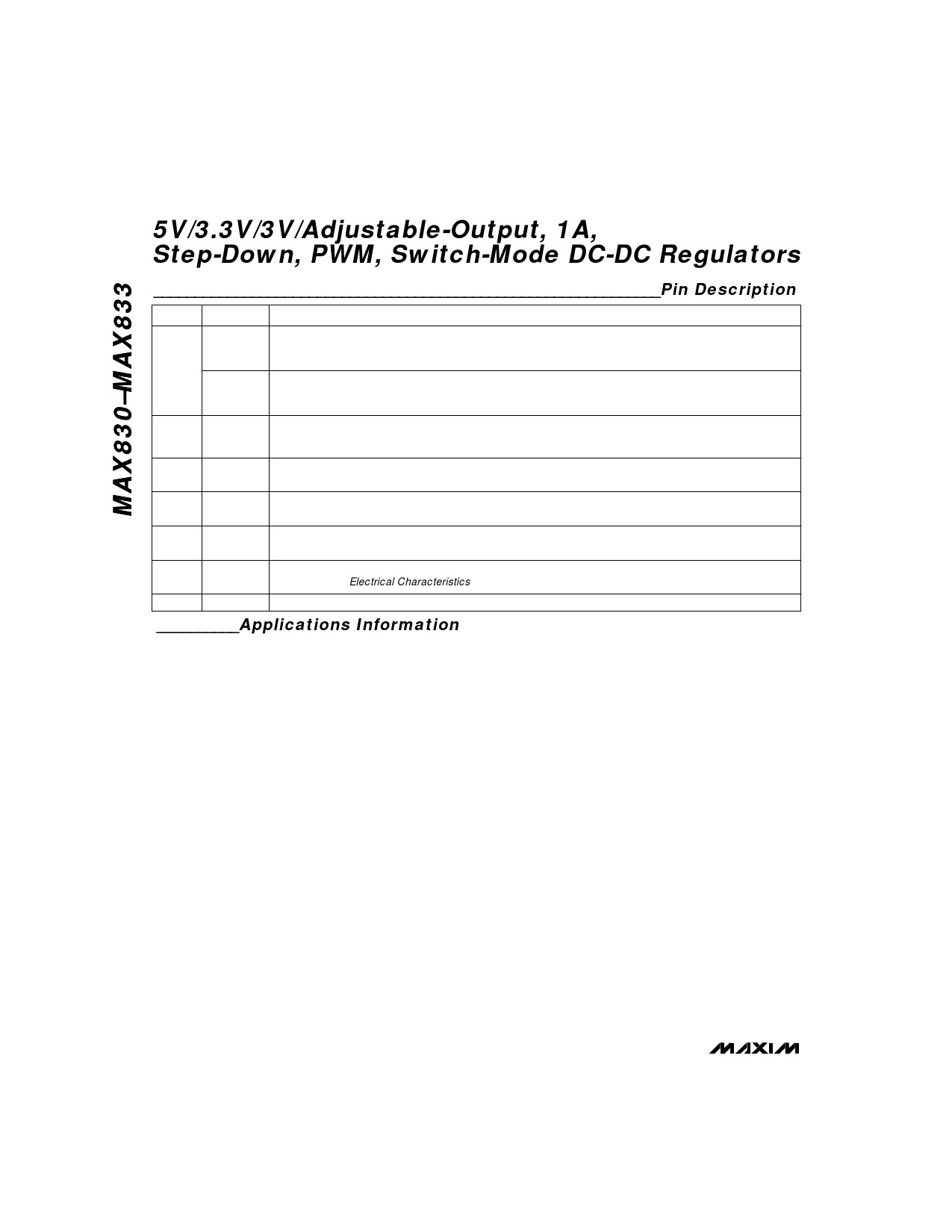
______________________________________________________________Pin Description
PIN
NAME
FUNCTION
SENSE For the MAX831/MAX832/MAX833, SENSE input is the internal error amplifier’s input, and should be
(MAX831/ directly connected to VOUT. SENSE also aids current limiting by reducing oscillator frequency when VOUT
2/3)
is low.
8
FB
(MAX830)
For the MAX830, the FB input is the internal error amplifier's input, and should be connected to the mid-
point of a potential divider between VOUT and GND (Figure 1). The output voltage, during regulation, will
be that value that forces 2.21V (VREF) at the FB pin.
Error-amplifier output. A series RC network connected to this pin compensates the device. Output swing
11
VC
is limited to about 5.8V in the positive direction and -0.7V in the negative direction. VC can also synchro-
nize the device to an external TTL clock in the 115kHz to 170kHz range.
5, 7,
10, 12
GND
Ground requires a short, low-noise connection to ensure good load regulation. The internal reference is referred
to GND, so errors at this pin are multiplied by the error amplifier. Use thick copper for low thermal resistance.
13, 14,
15, 16
VSW
Internal power switch output (rated for 1A load current)
1, 2,
3, 4
VIN
VIN supplies power to the internal circuitry and also connects to the collector of the internal power switch.
VIN must be bypassed with a low-ESR capacitor, typically 100µF.
6
ILIM
Switch-current limit can be reduced by connecting an external resistor (RLIM) from ILIM to GND
(See Note 7 in Electrical Characteristics). Leave ILIM floating for maximum current limit.
9
SHUT Shutdown is achieved by pulling SHUT low. Leave SHUT floating for normal operation.
__________Applications Information
Although the MAX830–MAX833 are high-efficiency
step-down voltage converters, certain precautions are
required to avoid excessive chip temperature (the
absolute maximum rating for this parameter, Tj, is
+125°C). The 16-pin SO package has thermal resis-
tance of +55°C/W when mounted properly; this limits
continuous chip power dissipation to the 1W range.
When installing these chips:
1) Use wide and, if possible, thick copper traces to
connect the leads (especially the GND pins) to
reduce thermal resistance.
2) Bond the package firmly to the board or use a clip-
style heatsink. A very small drop of thermal paste
between the chip package and the copper ground
plane is also helpful.
3) Confirm that the range of device operation is such
that the chip temperature does not exceed the
allowed maximum of Tj = +125°C. This can be
determined from Tables 1 and 2.
Tables 1 and 2 show numbers for maximum allowed
load current based on not exceeding the Tj = +125°C
limit. If the input voltage range, ambient temperature,
and/or output voltage setting allow for an unsafe level
of load current, limit the load current to a safe value by
connecting the appropriate resistor from the ILIM pin to
GND. With no external resistor, the preset switch cur-
rent limit (typically 1.7A) will limit the load current to
about 1.3A. Table 1 shows safe operating load cur-
rents for the MAX830 for various values of input and
output voltage and at three different ambient tempera-
tures of TA = +25°C, +45°C, and +70°C, respectively.
Table 2 shows the same information, but for the fixed
output voltage MAX831, MAX832, and MAX833.
When consulting these tables, note that power surges
of less than 30sec need not be considered from a ther-
mal standpoint. It is important for proper regulation,
however, that a power surge not require a peak switch
current exceeding the 1.2A (min) switch current limit.
Also, the inductor’s current rating should exceed IPEAK.
For highest efficiency, the inductor series resistance
should be 0.4Ω or less. IPEAK and ILOAD are related by
the following formula:
[VOUT x (VIN - VOUT)]
IPEAK = ILOAD + ——————————
VIN x L x 200,000
Example: MAX830 with VIN = 30V, VOUT = 15V,
ILOAD = 0.5A continuous, L = 100µH and
TA = +70°C:
IPEAK = 0.86A (which is below 1.2A (min)
preset switch current limit);
and from Table 1:
maximum ILOAD allowed = 0.8A continuous
(i.e., operation is safe).
4 _______________________________________________________________________________________
Share Link: