MAX9759(2005_10) View Datasheet(PDF) - Maxim Integrated
Part Name
Description
Manufacturer
MAX9759
(Rev.:2005_10)
(Rev.:2005_10)
Maxim Integrated

MAX9759 Datasheet PDF : 20 Pages
| |||
3.2W, High-Efficiency, Low-EMI,
Filterless, Class D Audio Amplifier
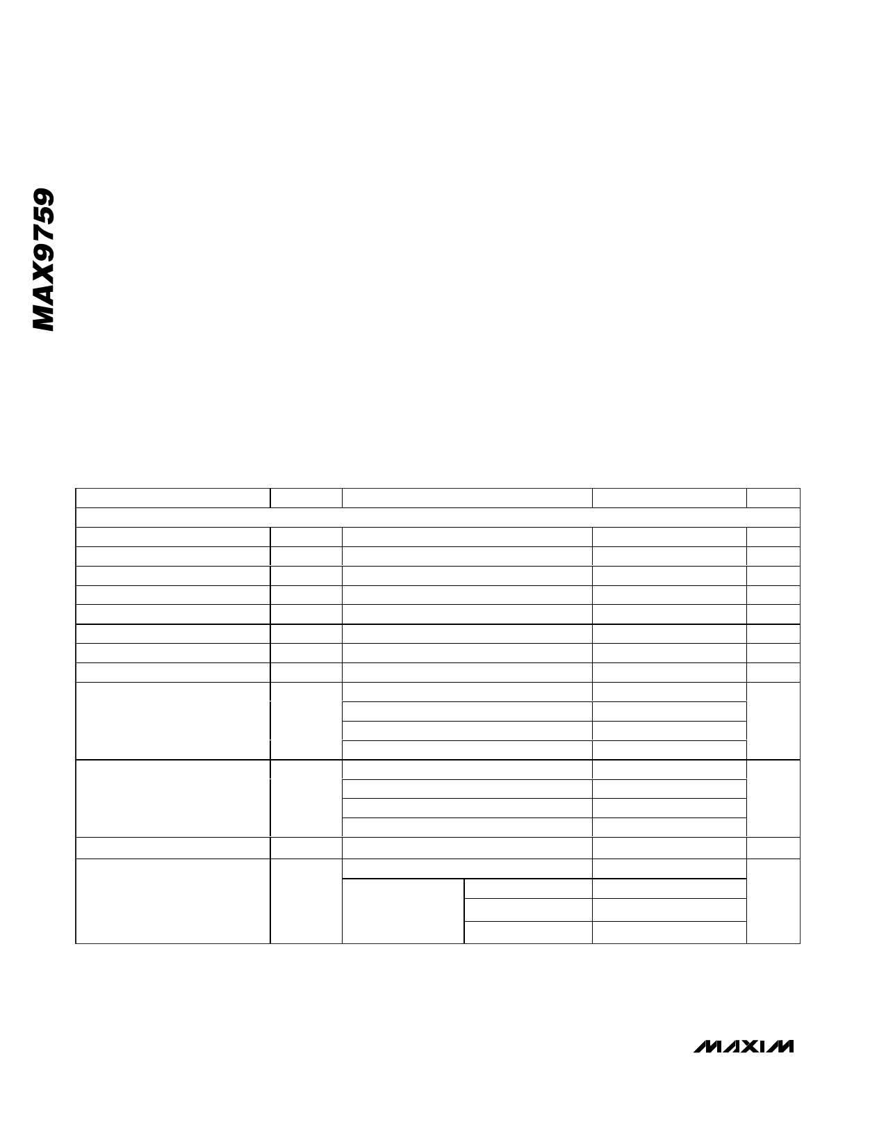
ABSOLUTE MAXIMUM RATINGS
VDD to GND..............................................................................6V
PVDD to PGND .........................................................................6V
GND to PGND .......................................................-0.3V to +0.3V
All Other Pins to GND.................................-0.3V to (VDD + 0.3V)
Continuous Current Into/Out of PVDD/PGND/OUT+/OUT-....1.7A
Duration of OUT+ or OUT- Short Circuit to
VDD/GND/PVDD/PGND............................................Continuous
Duration of Short Circuit Between OUT+ and OUT- ..Continuous
Continuous Power Dissipation (TA = +70°C)
16-Pin TQFN (derate 16.9mW/°C above +70°C) .....1349.1mW
Junction Temperature ......................................................+150°C
Operating Temperature Range ...........................-40°C to +85°C
Storage Temperature Range .............................-65°C to +150°C
Lead Temperature (soldering, 10s) .................................+300°C
ESD Protection (+IBM).........................................................±2kV
Stresses beyond those listed under “Absolute Maximum Ratings” may cause permanent damage to the device. These are stress ratings only, and functional
operation of the device at these or any other conditions beyond those indicated in the operational sections of the specifications is not implied. Exposure to
absolute maximum rating conditions for extended periods may affect device reliability.
ELECTRICAL CHARACTERISTICS (VDD = 5.0V)
(VDD = PVDD = SHDN = MUTE = 5V, GND = PGND = 0V, SYNC = 0V (FFM). Gain = 12dB (G1 = 0, G2 = 1). Speaker load resistor
(RL) connected between OUT+ and OUT-, unless otherwise noted, RL = ∞, TA = TMIN to TMAX, unless otherwise noted. Typical val-
ues are at TA = +25°C.) (Notes 1, 2)
PARAMETER
SYMBOL
CONDITIONS
MIN TYP MAX UNITS
GENERAL
Supply Voltage Range
Quiescent Current
Mute Current
Shutdown Current
Shutdown to Full Operation
Mute to Full Operation
Common-Mode Rejection Ratio
Input DC Bias Voltage
Input Resistance
Voltage Gain
VDD
IDD
IMUTE
IDD(SHDN)
tSON
tMUTE
CMRR
VCM
RIN
AV
Inferred from PSRR test
No load
V MUTE = 0V
V SHDN = 0V
f = 1kHz, input referred, VIN = 200mVP-P
Gain = +24dB
Gain = +18dB
Gain = +12dB
Gain = +6dB
G1 = 0, G2 = 0
G1 = 1, G2 = 0
G1 = 0, G2 = 1
G1 = 1, G2 = 1
3.0
5.5
V
8.4
12
mA
5.5
8
mA
0.1
10
µA
40
ms
40
ms
67
dB
1.3
1.5
1.7
V
14
20
26
25
36
47
kΩ
40
60
80
60
90
120
+22 +24 +26
+16 +18 +20
dB
+10 +12 +14
+4
+6
+8
Output Offset Voltage
Power-Supply Rejection Ratio
(Note 3)
VOS
PSRR
TA = +25°C
VDD = 4.5V to 5.5V
200mVP-P ripple
fRIPPLE = 217Hz
fRIPPLE = 1kHz
±10
±50
mV
62
90
79
dB
81
fRIPPLE = 20kHz
70
2 _______________________________________________________________________________________
Share Link: