MB84VD2119XA-85 View Datasheet(PDF) - Fujitsu
Part Name
Description
Manufacturer
MB84VD2119XA-85 Datasheet PDF : 55 Pages
| |||
MB84VD2118XA-85/MB84VD2119XA-85
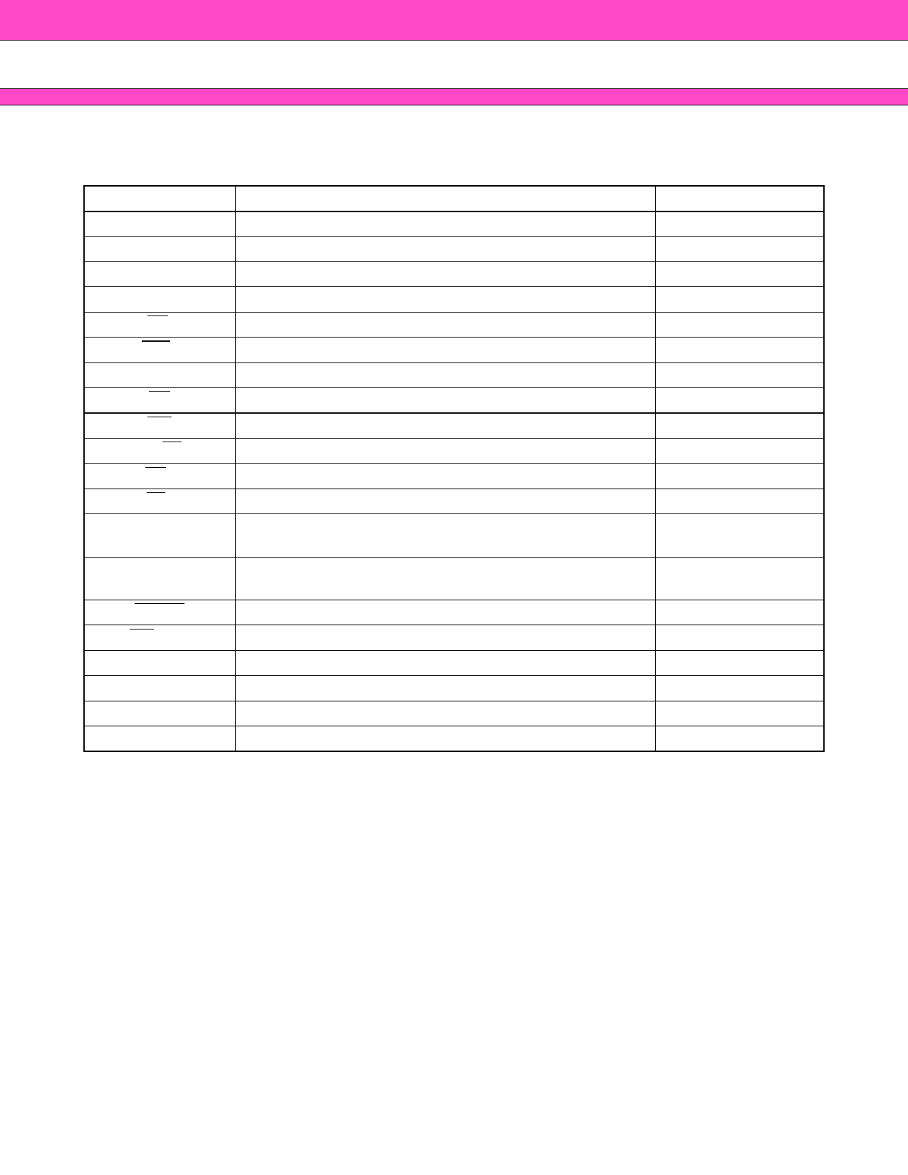
s PIN DESCRIPTION
Pin
A0 to A17
A-1, A18, A19
SA
DQ0 to DQ15
CEf
CE1s
CE2s
OE
WE
RY/BY
UBs
LBs
CIOf
CIOs
RESET
WP/ACC
N.C.
VSS
VCCf
VCCs
Function
Address Inputs (Common)
Address Input (Flash)
Address Input (SRAM)
Data Inputs/Outputs (Common)
Chip Enable (Flash)
Chip Enable (SRAM)
Chip Enable (SRAM)
Output Enable (Common)
Write Enable (Common)
Ready/Busy Outputs (Flash) Open Drain Output
Upper Byte Control (SRAM)
Lower Byte Control (SRAM)
I/O Configuration (Flash)
CIOf = VIH is Word mode ( √ó 16), CIOf = VIL is Byte mode ( √ó 8)
I/O Configuration (SRAM)
CIOs = VIH is Word mode ( √ó 16), CIOs = VIL is Byte mode ( √ó 8)
Hardware Reset Pin/Sector Protection Unlock (Flash)
Write Protect / Acceleration (Flash)
No Internal Connection
Device Ground (Common)
Device Power Supply (Flash)
Device Power Supply (SRAM)
Input/Output
I
I
I
I/O
I
I
I
I
I
O
I
I
I
I
I
I

Power
Power
Power
5
Share Link: 