MC13109FB View Datasheet(PDF) - Motorola => Freescale
Part Name
Description
Manufacturer
MC13109FB Datasheet PDF : 28 Pages
| |||
MC13109
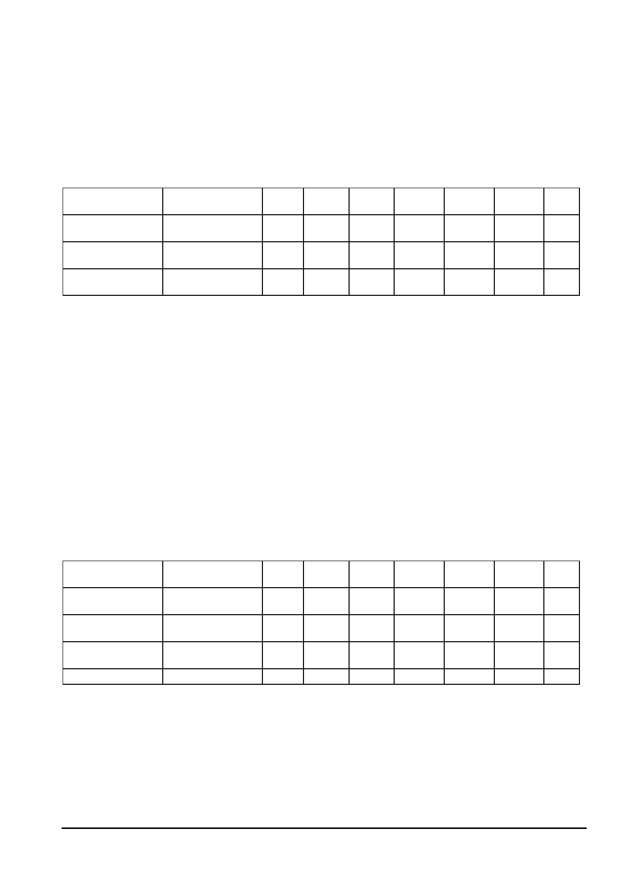
ELECTRICAL CHARACTERISTICS (continued)
Splatter Amplifier (see Figure 7)
The Splatter Amplifier is an inverting rail–to–rail output
operational amplifier with the non–inverting input terminal
connected to the internal VB half supply reference. External
resistors and capacitors can be connected to set the gain and
frequency response. The “Spl Amp In” input is ac coupled.
(Test Conditions: VCC = 2.6 V, TA = 25°C, fin = 1.0 kHz, External resistors Set for Gain of 1.)
Characteristic
Condition
Input Measure
Pin
Pin
Symbol
Min
Typ
Max
Unit
Open Loop Gain
–
Spl Amp Tx Out
AVOL
–
60
–
dB
In
Gain Bandwidth
–
Spl Amp Tx Out
GBW
–
100
–
kHz
In
Maximum Output
Swing
RL = 10 kΩ
Spl Amp Tx Out VOmax
–
VCC – 0.3
–
Vpp
In
Tx Audio Path Recommendation
The recommended configuration for the Tx Audio path
includes setting the Microphone Amplifier gain to 16 dB using
the external gain setting resistors and setting the Splatter
Amplifier gain to 9.0 dB using the external gain setting
resistors. With these gain values, the total Tx Path transfer
characteristic is shown in Figure 7.
PLL Voltage Regulator
The PLL supply voltage is regulated to a nominal of 2.2 V.
The “VCC Audio” pin is the supply voltage for the internal
voltage regulator. The “PLL Vref” pin is the 2.2 V regulated
output voltage. Two capacitors with 10 µF and 0.01 µF values
must be connected to the “PLL Vref” pin to filter and stabilize
this regulated voltage. The voltage regulator provides power
for the 2nd LO, Rx and Tx PLL’s, and MPU Interface. The
voltage regulator can also be used to provide a regulated
supply voltage for external IC’s. Rx and Tx PLL loop
performance are independent of the power supply voltage
when the voltage regulator is used. The voltage regulator
requires about 200 mV of “headroom”. When the power
supply decreases to within about 200 mV of the output
voltage, the regulator will go out of regulation but the output
voltage will not turn off. Instead, the output voltage will
maintain about a 200 mV delta to the power supply voltage as
the power supply voltage continues to decrease. The “PLL
Vref” pin can be connected to “VCC Audio” by the external
wiring if voltage higher than 2.2 V is required. But it should
not be connected to other supply except “VCC Audio”. The
voltage regulator is “on” in the Active and Rx modes. In the
Standby and Inactive modes, the voltage regulator is turned
off to reduce current drain and the “PLL Vref” pin is internally
connected to “VCC Audio” (i.e., the supply voltage is
maintained but is now unregulated).
(Test Conditions: VCC = 2.6 V, TA = 25°C.)
Characteristic
Condition
Input Measure
Pin
Pin
Symbol
Min
Output Voltge Level
VCC = 2.6 V,
OL= 0 mA
–
VCC PLL Vout
1.9
Line Regulation
IL = 0 mA, VCC = 2.6 to VCC VCC PLL Regline
–
5.5 V
Load Regulation
VCC = 2.6 V, IL = 0 to
VCC VCC PLL Regload
–
1.0 mA
Drop–Out Voltage
IL = 0 mA
–
–
DO
–
Typ
Max
Unit
2.2
2.5
V
1.43
40
mV
–1.86
40
mV
–
Vout + 200 mV
10
MOTOROLA ANALOG IC DEVICE DATA
Share Link: 