MC13142D View Datasheet(PDF) - Motorola => Freescale
Part Name
Description
Manufacturer
MC13142D Datasheet PDF : 16 Pages
| |||
MC13142
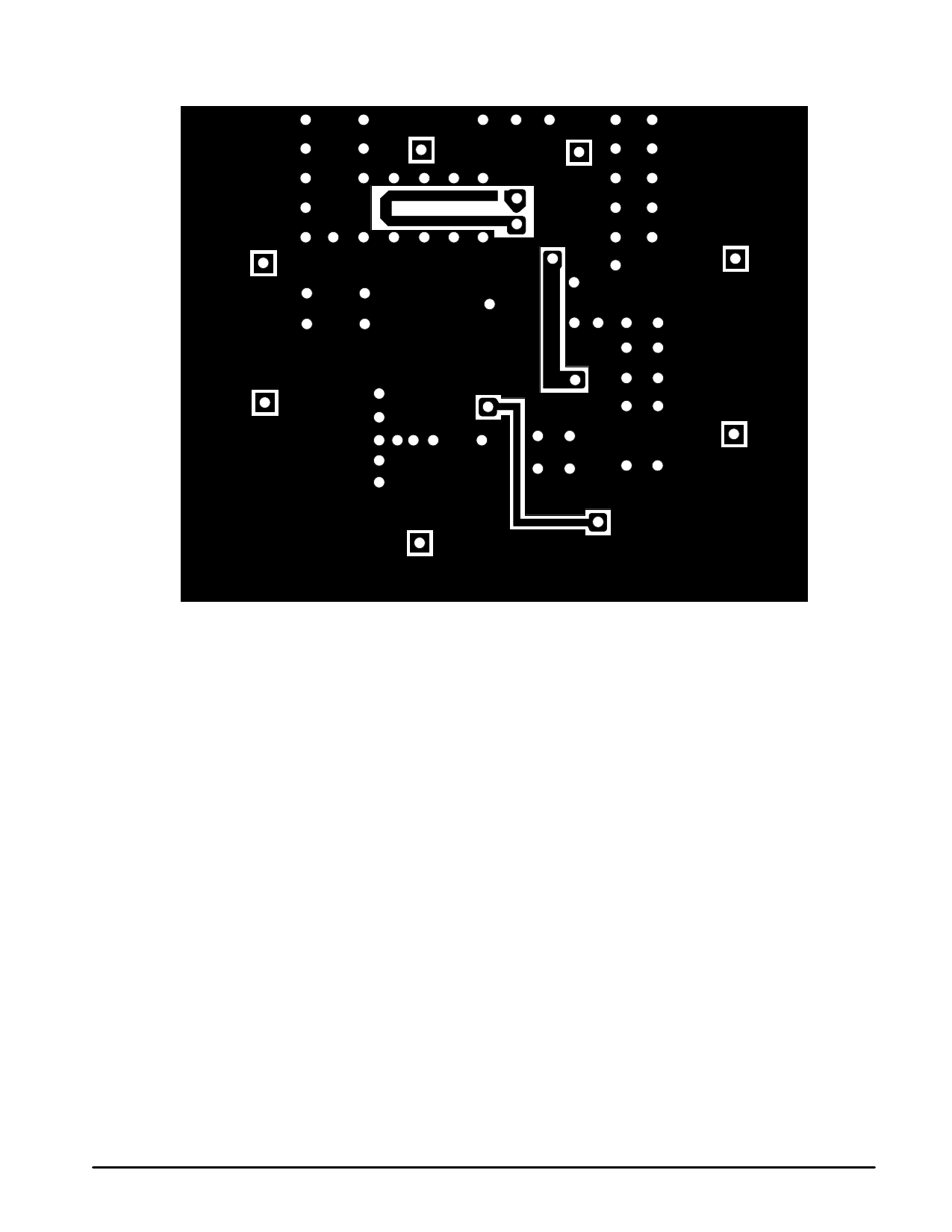
Figure 5. Ground Side View
V–Cont
VCC
LNA
Input
LO
Buf Out
LNA
Output
MC13142D
Rev A
NOTES: FR4 PCB, 1/32 inch.
Mix In
IF
Out
Mix Lin
Cont
1.9 GHz FRONT–END FOR WIRELESS SYSTEMS
This application is applicable to both Analog and Digital
systems. With the correct VCO tuning and the appropriate
filter, it will do the front–end for DECT, PHS or PCS. The
MC13142D is available in a SOIC 16 pin package. The part
requires minimal external components, leading to a low cost
system. A circuit board layout with a circuit diagram to
evaluate the IC is shown. Except for the PLL control, all the
wireless systems front–ends will look the same and have the
same basic performance characteristic as the test circuit.
Circuit Operation:
LNA Input/Output
An LC filter is incorporated before the LNA to provide
some selectivity. In addition to selectivity, its other function is
to match the antenna impedance (50 Ω) to the LNA input for
best gain and sensitivity (low noise figure). The network
reflects about a 200 Ω source impedance to the device.
The output circuit is a pie network consisting of; the LNA
output capacity, the inductance (the bond wire, package pin
and L2), and the input capacity of the dielectric filter, along
with some added shunt. A 2.4 pF with Toko 4DFA 2 pole filter.
The 2.4 pF is for matching the in–band filter impedance to the
LNA output and has little effect on tuning.
Both networks are tuned to band center by adjusting L1
and L2. L1 and L2, as well as L3, are short length of wire
formed in a half loop. Once the correct length is determined in
centering the tuning range, adjustment is accomplished by
moving the loop toward or away from some conductive
surface such as a ground plane.
The dielectric filter is referenced to the dc supply which
lessen the parts count and adds distributive capacity for high
frequency bypassing. DC feed to the LNA is through a low
value resistor (220 to 330 Ω) tapped at the filter input, so as not
to load the circuit unnecessarily. There is a small voltage drop
across the resistor, as well as some signal loss. The signal
loss is about 0.73 dB for a 220 Ω resistor and less for larger
values. If one can not afford the voltage drop, an inductor
could replace the resistor at a somewhat increased cost.
Mixer
Looking from the dielectric filter’s output, the Mixer input is
50 Ω in series with an inductor. This inductor consists of the
printed circuit run, the package pin and bond wire, all in
series. It is modified, to some extent, by the package pin
distributive capacity, but overall at the bandpass frequency
remains inductive. Matching the filter impedance to the Mixer
input only requires a capacitor with a value that, when placed
in series, will resonate with this inductor at the filter bandpass
frequency.
The single–ended input signal is converted internally into
balanced current signals. The two signals drive the two low
impedance inputs (emitters) of a Gilbert Cell. They appear as
10
MOTOROLA RF/IF DEVICE DATA
Share Link: 