MC13156FB View Datasheet(PDF) - Motorola => Freescale
Part Name
Description
Manufacturer
MC13156FB Datasheet PDF : 20 Pages
| |||
MC13156
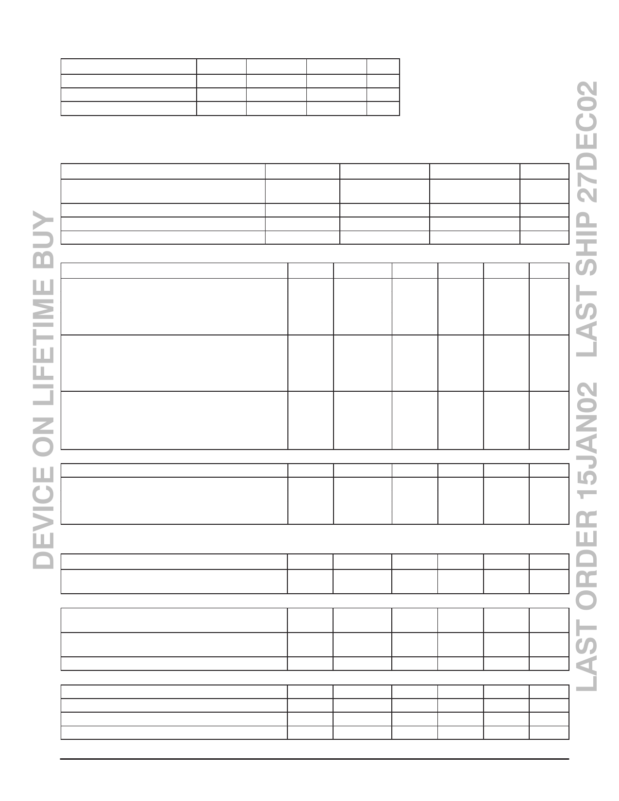
MAXIMUM RATINGS
Rating
Pin
Symbol
Value
Unit
Power Supply Voltage
Junction Temperature
Storage Temperature Range
16, 19, 22
–
–
VEE(max)
TJ(max)
Tstg
–6.5
Vdc
150
°C
–65 to +150
°C
NOTES: 1. Devices should not be operated at or outside these values. The “Recommended Operating
Conditions” table provides for actual device operation.
2. ESD data available upon request.
RECOMMENDED OPERATING CONDITIONS
Rating
Pin
Symbol
Power Supply Voltage @ TA = 25°C
–40°C ≤ TA ≤ +85°C
Input Frequency
Ambient Temperature Range
Input Signal Level
4, 9
16, 19, 22
1, 2
–
1, 2
VCC
VEE
fin
TA
Vin
DC ELECTRICAL CHARACTERISTICS (TA = 25°C, VCC1 = VCC2 = 0, no input signal.)
Characteristic
Pin
Symbol
Min
Total Drain Current (See Figure 2)
VEE = –2.0 Vdc
VEE = –3.0 Vdc
VEE = –5.0 Vdc
VEE = –6.0 Vdc
Drain Current, I22 (See Figure 3)
VEE = –2.0 Vdc
VEE = –3.0 Vdc
VEE = –5.0 Vdc
VEE = –6.0 Vdc
Drain Current, I19 (See Figure 3)
VEE = –2.0 Vdc
VEE = –3.0 Vdc
VEE = –5.0 Vdc
VEE = –6.0 Vdc
19, 22
ITotal
–
3.0
–
–
22
I22
–
–
–
–
19
I19
–
–
–
–
DATA SLICER (Input Voltage Referenced to VEE = –3.0 Vdc, no input signal; See Figure 15.)
Input Threshold Voltage (High Vin)
15
V15
1.0
Output Current (Low Vin)
Data Slicer Enabled (No Hold)
17
I17
–
V15 > 1.1 Vdc
V18 = 0 Vdc
Value
0 (Ground)
–2.0 to –6.0
500
–40 to +85
200
Typ
Max
4.8
–
5.0
8.0
5.2
–
5.4
–
3.0
–
3.1
–
3.3
–
3.4
–
1.8
–
1.9
–
1.9
–
2.0
–
1.1
1.2
1.7
–
AC ELECTRICAL CHARACTERISTICS (TA = 25°C, VEE = –3.0 Vdc, fRF = 130 MHz, fLO = 140.7 MHz, Figure 1 test
circuit, unless otherwise specified.)
Characteristic
12 dB SINAD Sensitivity (See Figures 17, 25)
fin = 144.45 MHz; fmod = 1.0 kHz; fdev = ±75 kHz
MIXER
Conversion Gain
Pin = –37 dBm (Figure 4)
Mixer Input Impedance
Single–Ended (Table 1)
Mixer Output Impedance
IF AMPLIFIER SECTION
IF RSSI Slope (Figure 6)
IF Gain (Figure 5)
Input Impedance
Output Impedance
Pin
Symbol
Min
Typ
Max
1, 14
–
–
–100
–
1, 3
–
1, 2
Rp
Cp
3
–
20
–
5, 8
–
5
–
8
–
–
22
–
–
1.0
–
–
4.0
–
–
330
–
0.2
0.4
0.6
–
39
–
–
1.4
–
–
290
–
Unit
Vdc
MHz
°C
mVrms
Unit
mA
mA
mA
Vdc
mA
Unit
dBm
dB
kΩ
pF
Ω
µA/dB
dB
kΩ
Ω
2
MOTOROLA WIRELESS SEMICONDUCTOR
SOLUTIONS – RF AND IF DEVICE DATA
Share Link: 