MC13110AFB View Datasheet(PDF) - Motorola => Freescale
Part Name
Description
Manufacturer
MC13110AFB Datasheet PDF : 68 Pages
| |||
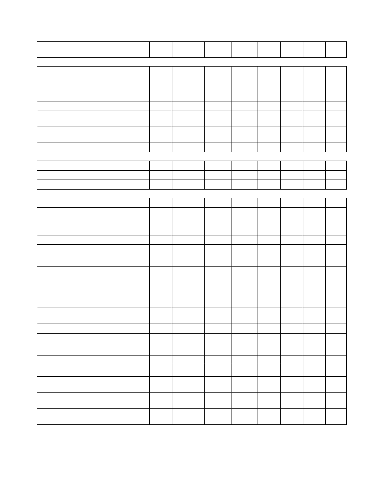
MC13110A/B MC13111A/B
ELECTRICAL CHARACTERISTICS (continued) (VCC = 3.6 V, VB = 1.5 V, TA = 25°C, Active or Rx Mode, unless otherwise specified;
Test Circuit Figure 1.)
Characteristic
Figure
Input
Pin
Measure
Pin
Symbol Min
Typ
Max Unit
DATA AMP COMPARATOR
Hysteresis
1
DA In
DA Out
Hys
30
42
50
mV
Threshold Voltage
–
DA In
DA Out
VT
–
VCC –
–
V
0.7
Input Impedance
1
–
DA In
ZI
200
250
280
kΩ
Output Impedance
–
–
DA Out
ZO
–
100
–
kΩ
Output High Voltage
Vin = VCC – 1.0 V, IOH = 0 mA
1
DA In
DA Out
VOH VCC – 3.6
–
V
0.1
Output Low Voltage
Vin = VCC – 0.4 V, IOL = 0 mA
1
DA In
DA Out
VOL
–
0.1
0.4
V
Maximum Frequency
–
DA In
DA Out
Fmax
–
10
–
kHz
MIC AMP (fin = 1.0 kHz, External resistors set to gain of 1, Active Mode)
Open Loop Gain
–
Tx In
Amp Out AVOL
– 100,000 –
V/V
Gain Bandwidth
–
Tx In
Amp Out GBW
–
100
–
kHz
Maximum Output Swing (RL = 10 kΩ)
–
Tx In
Amp Out VOmax
–
3.2
–
Vpp
Tx AUDIO PATH (fin = 1.0 kHz, Tx Gain Adj = (01111); ALC, Limiter, and Mutes Disabled; Active Mode, scrambler bypassed)
Absolute Gain (Vin = –10 dBV)
1, 83
Tx In
Tx Out
G
–4.0
0
4.0
dB
Gain Tracking
(Referenced to Tx Out for Vin = –10 dBV)
Vin = – 30 dBV
Vin = – 40 dBV
1, 87
Tx In
Tx Out
Gt
dB
–11
–10
–9.0
–17
–15
–13
Total Harmonic Distortion (Vin = – 10 dBV)
1, 87
Tx In
Tx Out
THD
–
0.8
1.8
%
Maximum Output Voltage (Increase input voltage
1
until output voltage THD = 5.0%, then measure
output voltage. Tx Gain Adjust = 8 dB)
Tx In
Tx Out VOmax –2.0
0
–
dBV
Input Impedance
–
–
C In
Zin
–
10
–
kΩ
Attack Time (Ccap = 0.5 µF, Rfilt = 40 k (See
Appendix B))
–
C In
Tx Out
ta
–
3.0
–
ms
Release Time (Ccap = 0.5 µF, Rfilt = 40 k (See
–
Appendix B))
C In
Tx Out
tr
–
13.5
–
ms
Expander to Compressor Crosstalk (Vin = –20 dBV,
Speaker Amp No Load, V(C In) = AC Gnd)
Tx Muting (Vin – 10 dBV)
ALC Output Level (ALC enabled)
Vin = –10 dBV
Vin = –2.5 dBV
ALC Slope (ALC enabled)
Vin = –10 dBv
Vin = –2.5 dBv
ALC Input Dynamic Range
1
1
1, 87,
90
1
–
E In
Tx In
Tx In
Tx In
C In
Tx Out
CT
–
–60
–40
dB
Tx Out
Mc
–
–88
–60
dB
Tx Out ALCout
dBV
–15
–13
–8.0
–13
–11
–6.0
Tx Out
Slope
0.1
0.25
0.4 dB/dB
Tx Out
DR
–
–16 to
–
dBV
–2.5
Limiter Output Level (Vin = – 2.5 dBV,
Limiter enabled)
1
Tx In
Tx Out
Vlim
–10
–8.0
–
dBV
Tx High Frequency Corner [Note 7]
(VTx In = –10 dBV, Mic Amp = Unity Gain)
1
Tx In
Tx Out
Tx fc
3.6
3.7
3.8
kHz
NOTE: 7. The filter specification is based on a 10.24 MHz 2nd LO, and a switched–capacitor (SC) filter counter divider ratio of 31. If other 2nd LO frequencies
and/or SC filter counter divider ratios are used, the filter corner frequency will be proportional to the resulting SC filter clock frequency.
MOTOROLA ANALOG IC DEVICE DATA
7
Share Link: 